Multi-layer high gradient insulator and manufacturing method thereof

An insulator, high-gradient technology, applied in the direction of insulators, suspension/strain insulators, electrical components, etc., can solve the problems of difficult molding process, high flashover voltage, poor mechanical properties, etc., to improve the vacuum surface flashover characteristics, flashover The effect of high network voltage and overcoming poor mechanical properties

Active Publication Date: 2013-08-14
NORTHWEST INST OF NUCLEAR TECH
View PDF3 Cites 15 Cited by
  • Summary
  • Abstract
  • Description
  • Claims
  • Application Information

AI Technical Summary

Problems solved by technology

[0005] The present invention designs a high-gradient insulator with an insulating material / conductive layer alternate lamination structure on the surface of the insulating working surface and its preparation method, which not only utilizes the advantages of high flashover voltage along the surface of general multi-layer high-gradient insulators, but also overcomes the The original multi-layer high gradient insulator has the defects of poor mechanical properties, difficult forming process and high cost

Method used


Image

  • Multi-layer high gradient insulator and manufacturing method thereof
  • Multi-layer high gradient insulator and manufacturing method thereof
  • Multi-layer high gradient insulator and manufacturing method thereof

Examples


Embodiment 1

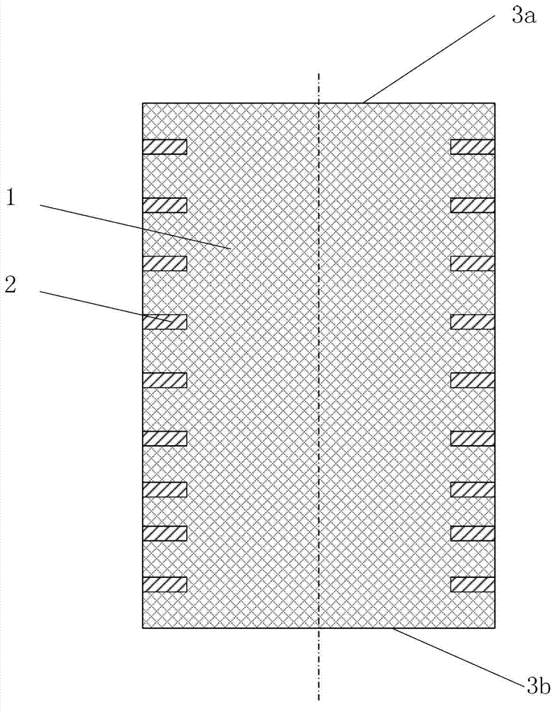
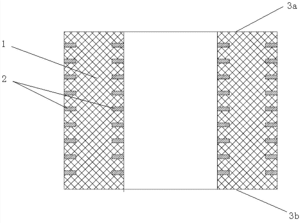
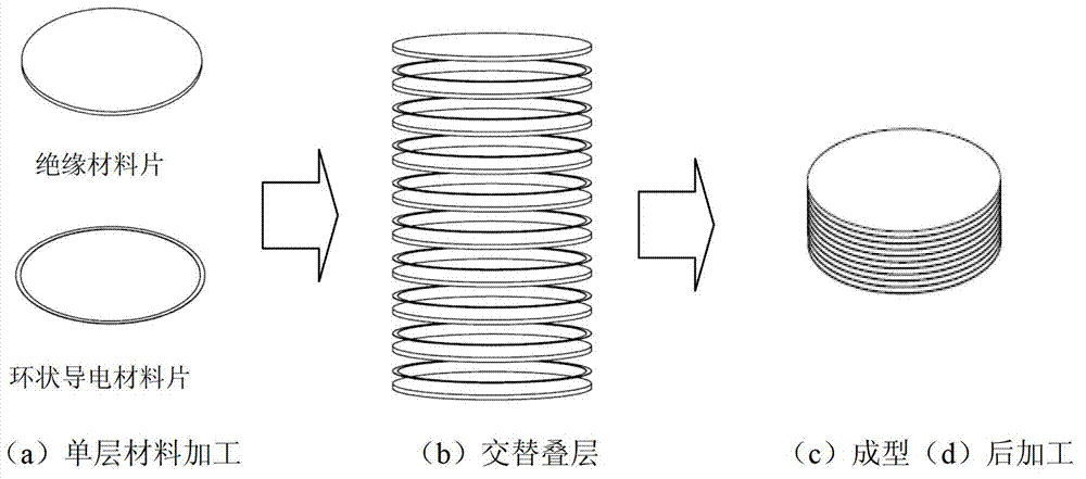
[0048] 1) With 1mm thick polystyrene (PS) sheet as the insulating material and 0.02mm thick stainless steel foil as the conductive material, the PS sheet is cut into Ф40.0mm discs, and the stainless steel foil is cut into outer diameter 40.0mm, wide 1.0mm circular ring; 2) Alternately stack the above PS discs and stainless steel rings one by one, with a total of 10 layers of PS and 9 layers of stainless steel rings, and put them into a mold with an inner diameter of 40.1mm; 3) Put the above mold and materials into In the hot pressing device, heat to 180°C and keep it warm for 2 hours to fully melt the PS material, apply a pressure of 1 MPa on the mold, and heat and solidify the multi-layer materials in the mold; 4) Grind the side of the formed insulator to remove the surface layer Defects, that is, to obtain a multi-layer high-gradient insulator with a total thickness of about 10mm, see the process image 3 .

Embodiment 2

[0050] 1) Use 0.2mm thick polyimide (PI) sheet as the insulating material and 0.01m thick stainless steel foil as the conductive material, cut the PI sheet into Ф40.0mm discs, and cut the stainless steel foil into 40.0mm outer diameter , a ring with a width of 1.0mm; 2) Alternately stack the above-mentioned PI discs and stainless steel rings one by one, with a total of 50 layers of PI and 49 layers of stainless steel rings, and put them into a mold with an inner diameter of 40.1mm; 3) Put the above-mentioned mold and materials Put it into the hot pressing device, heat it to 430°C and keep it warm for 2 hours to fully soften the PI material, apply a pressure of 30MPa on the mold, and heat and solidify the multi-layer material in the mold; 4) Grind the side of the formed insulator to remove Surface layer defects, that is, a multi-layer high-gradient insulator with a total thickness of about 10 mm is obtained. see process image 3 .

Embodiment 3

[0052] 1) Use 1mm thick polystyrene (PS) sheet as the insulating material, cut the PS sheet into Ф40.0mm discs; 2) Use low-temperature cured silver paste as the conductive material, and print on the PS disc by screen printing A ring with an outer diameter of 40.0mm, a width of 1.0mm, and a thickness of 0.01mm, and dried at 100°C; 3) Stack the above-mentioned PS wafers printed with conductive rings layer by layer, a total of 10 layers, and put them into the inner hole with a diameter of 40.1mm In the mold; 4) Put the above mold and materials into the hot pressing device, heat to 180°C and keep it warm for 2 hours to fully melt the PS material, apply a pressure of 1MPa on the mold, and heat and solidify the multi-layer materials in the mold; 5 ) Grind the side of the formed insulator to remove surface layer defects, and obtain a multi-layer high-gradient insulator with a thickness of about 10 mm. see process Figure 4 .


PUM

PropertyMeasurementUnit
thicknessaaaaaaaaaa

Abstract

The invention discloses a multi-layer high gradient insulator for a high-voltage pulse power supply and a manufacturing method thereof. The multi-layer high gradient insulator is characterized in that thin conductive layers are regularly embedded in an insulator body made of an insulated material, the side surface of the insulator, which is in a certain depth, is formed by an insulated material layer and a conductive material layer, and the interior of the insulator is formed by a single insulated material. According to the invention, a conductive array is embedded in the side surface of the insulator body, the secondary electron emitting characteristic of the surface of the insulator and the surface load charge accumulation are restrained, the vacuum surface flashover characteristic of the insulator body is improved, the surface impact voltage of the insulator body is improved, the problem that the insulated material layer is not matched with the mechanical and thermal performance of the conductive material layer is solved, and the process difficulty and cost for manufacturing the multi-layer high gradient insulator are remarkably lowered.

Description

technical field [0001] The invention belongs to the technical field of high-voltage insulation, and in particular relates to a multilayer high-gradient insulator with excellent vacuum insulation performance and a preparation process thereof. Background technique [0002] An insulator is a component used for electrical insulation and mechanical fixing. Its function is to connect conductors with different potentials to each other mechanically and to insulate them electrically. With the development of science and technology, the surface flashover phenomenon of insulators has become a prominent problem in vacuum electrical equipment. Surface flashover makes the withstand voltage capacity of insulators far lower than its bulk breakdown voltage, and is much lower than that of vacuum at the same distance. gap. With the increasingly prominent role of high-power pulse technology in national economy and national defense construction, many large-scale cutting-edge equipment, such as h...

Claims


Application Information

Patent Timeline
Patent Type & Authority Applications(China)
IPC IPC(8): H01B17/04H01B17/50
Inventor 柯昌凤刘文元陈昌华宋玮汤俊平段荔薛西民
Owner NORTHWEST INST OF NUCLEAR TECH
Why Eureka
Try Eureka