On-chip ferrite bead inductor

A ferrite bead, inductor technology, applied in inductors, electro-solid devices, semiconductor devices, etc., can solve the problems of integration incompatibility, consumption of substrate surface, large form factor, etc.

Active Publication Date: 2013-08-14
TAIWAN SEMICON MFG CO LTD
View PDF3 Cites 8 Cited by
  • Summary
  • Abstract
  • Description
  • Claims
  • Application Information

AI Technical Summary

Problems solved by technology

Therefore, when mounted on a PCB, SMD ferrite beads have a relatively large form factor and consume useful real estate
SMD ferrite bead

Method used


Image

  • On-chip ferrite bead inductor
  • On-chip ferrite bead inductor
  • On-chip ferrite bead inductor

Examples


Embodiment Construction

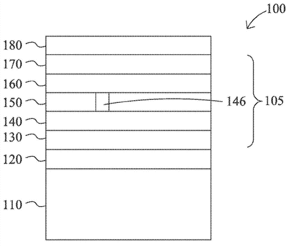
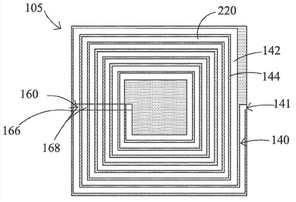
[0034] expected combination Figure 1 This description of exemplary embodiments should be read in conjunction with the accompanying drawings, which are considered a part of the entire written description. In the description of the embodiments disclosed herein, any reference to direction or orientation is intended for convenience of description purposes only and is not intended to limit the scope of the invention in any way. Relative terms such as "lower", "upper", "horizontal", "vertical", "above", "below", "upward", "downward", "top" and "bottom" and their derivatives (e.g., "Horizontally", "downwardly", "upwardly", etc.) should be construed to mean an orientation as described subsequently or as shown in the drawings in the discussion. These relative terms are for convenience of description only and do not require that the device be constructed or operated in a particular orientation. Unless expressly stated otherwise, terms relating to joining, connecting, etc. (such as "c...


PUM


Abstract

A semiconductor structure having an in situ chip-level ferrite bead inductor and method for forming the same. Embodiments include a substrate, a first dielectric layer formed on the substrate, a lower ferrite layer formed on the first dielectric layer, and an upper ferrite layer spaced apart from the lower ferrite layer in the structure. A first metal layer may be formed above the lower ferrite layer and a second metal layer formed below the upper ferrite layer, wherein at least the first or second metal layer has a coil configuration including multiple turns. At least one second dielectric layer may be disposed between the first and second metal layers. The ferrite bead inductor has a small form factor and is amenable to formation using BEOL processes.

Description

technical field [0001] The present invention relates generally to semiconductor structures and, more particularly, to semiconductor structures including integrated passive devices (IPDs), such as ferrite bead inductors, and methods of forming the same. Background technique [0002] A major trend in semiconductor manufacturing today is the integration of 2.5D and 3DIC chip or die packages with vertically stacked chips and direct electrical connections between chips instead of other interconnect technologies such as wire bonding and chip edge interconnect. The dies in these IC chip packages may include fine (small) pitch vertical through-substrate vias (TSVs), which may be used to make direct electrical connections to adjacent stacked dies. TSVs provide higher density interconnects and shorter signal paths, creating the possibility to form die packages with smaller form factors and thin die stacks. The TSVs in the top die can be terminated on the backside of an array of micro...

Claims


Application Information

Patent Timeline
IPC IPC(8): H01L23/522H01L21/02
CPCH01L2924/0002H01L28/10H01L23/5227H01L23/645H01L2924/00
Inventor 金俊德叶子祯
Owner TAIWAN SEMICON MFG CO LTD
Why Eureka
Try Eureka