Check patentability & draft patents in minutes with Patsnap Eureka AI!

NVM (nonvolatile memory) component and array thereof

A technology for memory components and memory arrays, applied in the field of electronic components and their arrays, can solve the problems of increasing the reading current value, reducing the reading margin, reading, etc.

Inactive Publication Date: 2013-08-14
WINBOND ELECTRONICS CORP
View PDF4 Cites 4 Cited by
  • Summary
  • Abstract
  • Description
  • Claims
  • Application Information

AI Technical Summary

Problems solved by technology

The existence of this path will make the leakage current flow through the word line WL2 and the bit line BL2 along the adjacent memory cells. At this time, the value of the read current will increase abnormally, thereby significantly reducing the read margin. cause the wrong bit state to be read

Method used


Image

  • NVM (nonvolatile memory) component and array thereof
  • NVM (nonvolatile memory) component and array thereof
  • NVM (nonvolatile memory) component and array thereof

Examples


Embodiment Construction

[0033] Embodiments of the present invention solve the leakage current problem by adding a non-linear element to the memory cell and connecting it in series with the internal resistance element. Such a non-linear element is, for example, a unipolar diode, which is connected in series with a unipolar resistance element to increase the non-linearity of the resistance value in the low resistance state. Its structure is 1D1R in the embodiment of the present invention. structure as an example. In addition, if in order to maintain 4F 2 The minimum unit cell size, the resistance element and the diode element can be stacked vertically (vertically stacked) to achieve the purpose of series connection. Therefore, it is beneficial to be applied to high-density non-volatile memory.

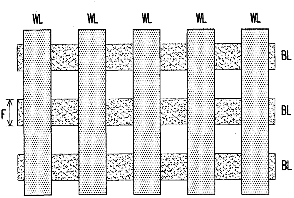
[0034] The present invention is described in detail below with an embodiment and drawings. image 3 It is a schematic diagram of a three-dimensional structure of a non-volatile memory array according to an e...


PUM


Abstract

An NVM (nonvolatile memory) component comprises a first electrode, a resistance structure, a diode structure and a second electrode, wherein the resistance structure is configured on the first electrode, and comprises a first oxide layer; the first oxide layer is configured on the first electrode; the diode structure is configured on the resistance structure, and comprises a metal layer and a second oxide layer; the metal layer is configured on the first oxide layer; the second oxide layer is configured on the metal layer; the second electrode is configured on the diode structure; and the metal layer and the second electrode are made of different materials. In addition, the invention also provides an NVM array including the NVM component.

Description

technical field [0001] The present invention relates to an electronic component and its array, and in particular to a non-volatile memory component and its array. Background technique [0002] Recently, resistive random access memory (RRAM) has been widely used in the technical field of non-volatile memory due to its simple crossbar array structure and low-temperature manufacturing process. The architecture of this crossbar array is designed based on the concept of resistive-switching elements, which theoretically can obtain the smallest cell size (cell size) 4F 2 , where F represents the feature size (feature size). Therefore, the interleaved nonvolatile memory array can have a relatively high integration density. [0003] figure 1 It is a conceptual schematic diagram of the unit cell size of the prior art. exist figure 1 Among them, the nonvolatile memory array is composed of a plurality of bit lines BL and word lines WL, and the cross-point of the two is where the me...

Claims


Application Information

Patent Timeline
IPC IPC(8): H01L27/102H01L27/10
Inventor 侯拓宏黄俊嘉
Owner WINBOND ELECTRONICS CORP
Features
  • R&D
  • Intellectual Property
  • Life Sciences
  • Materials
  • Tech Scout
  • Unparalleled Data Quality
  • Higher Quality Content
  • 60% Fewer Hallucinations
Learn More