Active type OLED (organic light-emitting diode) display device and manufacturing method thereof
A display device, active technology, applied in semiconductor/solid-state device manufacturing, electric solid-state devices, semiconductor devices, etc., can solve the problems of low contact resistance of cathode and cathode power supply lines, light output rate and process are not easy to achieve, etc. The effect of extraction rate, reduction of contact resistance, and simple preparation process
- Summary
- Abstract
- Description
- Claims
- Application Information
AI Technical Summary
Problems solved by technology
Method used
Image
Examples
Embodiment 1
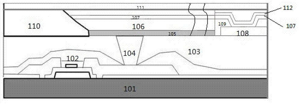
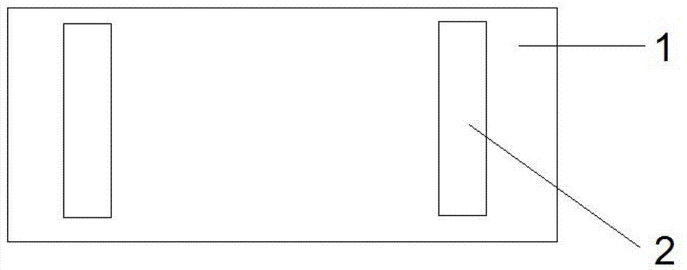
[0036] The active OLED display device provided by this embodiment, as attached figure 1 As shown, an OLED pixel unit is included, wherein the OLED pixel unit includes at least two TFTs 102, an anode 105 disposed on the TFT 102, a cathode 107 disposed opposite to the anode 105, and an organic functional layer 106 disposed between the anode 105 and the cathode 107, The active OLED display device also includes a cathode power supply line 108, and an insulating layer 109 arranged between the cathode 107 and the cathode power supply line 108, the insulating layer 109 is provided with a contact hole for conducting the cathode 107 and the cathode power supply line 108, and the cathode 107 is provided with a cathode thickening layer 112 with a thickness of 30nm, and the cathode thickening layer 112 is only flatly arranged on the positive projection area of the cathode power line 108 on the cathode 107, such as image 3 shown.
[0037] The TFT 102 in this embodiment is preferably a ...
Embodiment 2
[0050] This embodiment provides an active OLED display device. The specific structure and preparation method of the device are the same as those in Embodiment 1. The only difference is that the structure of the open mask in step 3 is different, and the opening area of the open mask corresponds to the cathode 107 and In the contact hole area of the cathode power line, the cathode thickening layer 112 is evenly arranged on the positive projection area of the contact hole on the cathode 107, such as Figure 4 shown.
[0051] The thickness of each functional layer in this embodiment can be changed according to the structure and application of the specific display device, and it is not necessary and impossible to exhaustively list all the implementation modes here, and the obvious changes or changes derived from this are still in the scope of the present invention. within the scope of protection.
PUM
 Abstract
Description
Claims
Application Information


