Bidirectional and symmetrical high-speed overvoltage protective device

A technology for overvoltage protection devices and devices, which is applied in the fields of electric solid state devices, semiconductor devices, semiconductor/solid state device components, etc., to achieve the effect of improving protection capability, superiority and capability.

Active Publication Date: 2013-08-21
BEIJING YANDONG MICROELECTRONICS +1
View PDF3 Cites 8 Cited by
  • Summary
  • Abstract
  • Description
  • Claims
  • Application Information

AI Technical Summary

Problems solved by technology

[0006] In order to achieve this goal, the technical solution adopted by the present invention is: in view of the structural defects of the current mainstream semiconductor overvoltage protection device, such as the overvoltage protection device of the model TisP61089B available in the market, replace the positive overvoltage protection with a thyristor. Diode, so as to form a combination of NPN transistor and NPNP thyristor controlled by it for negative overvoltage protection, and a combination of PNP transistor and PNPN thyristor controlled by it for positive overvoltage protection. The combination of the two forms a Both positive a...

Method used


Image

  • Bidirectional and symmetrical high-speed overvoltage protective device
  • Bidirectional and symmetrical high-speed overvoltage protective device
  • Bidirectional and symmetrical high-speed overvoltage protective device

Examples


Embodiment 1

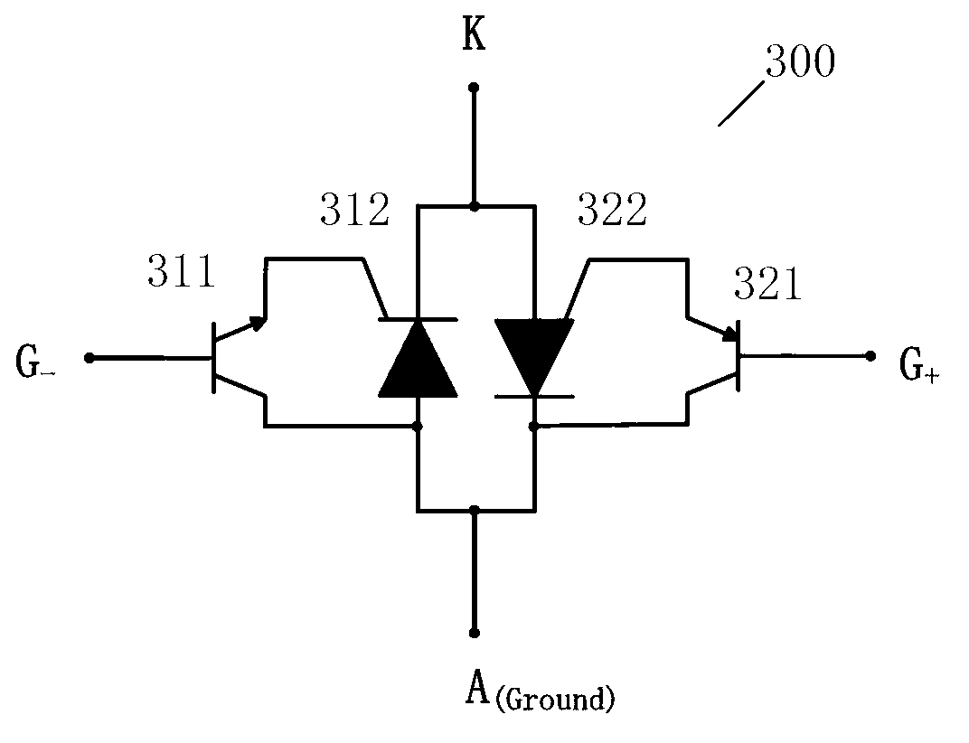
[0072] image 3 A schematic diagram of an overvoltage protection circuit 300 according to Embodiment 1 of the present invention is shown. The overvoltage protection circuit 300 includes an NPN transistor 311 and an NPNP thyristor 312 as well as a PNP transistor 321 and a PNPN thyristor 322 . The emitter and the collector of the NPN transistor 311 are respectively connected to the control electrode and the anode of the NPNP transistor 312 , and the emitter and the collector of the PNP transistor 321 are respectively connected to the control electrode and the cathode of the PNPN transistor 322 . The base of the NPN transistor 311 is used as the negative overvoltage reference potential port G of the protection circuit – , the base of the PNP transistor 321 serves as the forward overvoltage reference potential port G of the protection circuit + . The anode of the NPNP thyristor 312 and the cathode of the PNPN thyristor 322 are connected as the ground port A (Ground) of the prot...

Embodiment 2

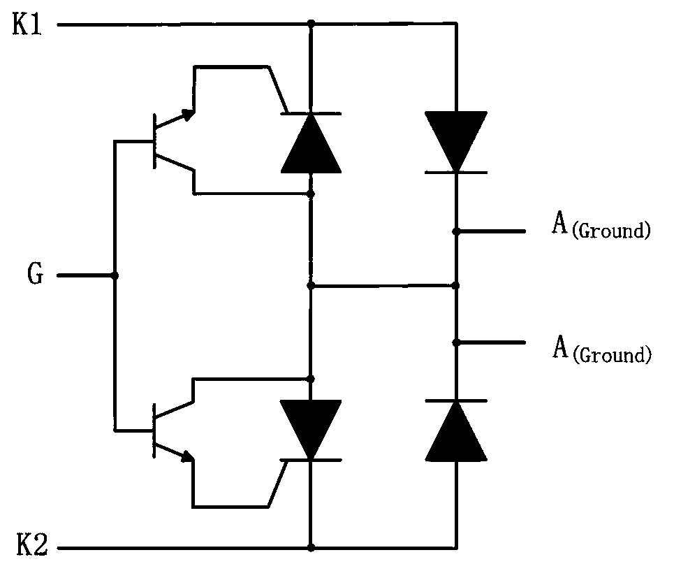
[0075] Figure 4 A schematic diagram of an overvoltage protection circuit 400 according to Embodiment 2 of the present invention is shown. The overvoltage protection circuit 400 includes a first protection unit and a second protection unit, and each protection unit has image 3 structure shown. The first protection unit includes an NPN transistor 411 and an NPNP thyristor 412 and a PNP transistor 421 and a PNPN thyristor 422 . The emitter and the collector of the NPN transistor 411 are respectively connected to the control electrode and the anode of the NPNP transistor 412 , and the emitter and the collector of the PNP transistor 421 are respectively connected to the control electrode and the cathode of the PNPN transistor 422 . The second protection unit includes an NPN transistor 431 and an NPNP thyristor 432 and a PNP transistor 441 and a PNPN thyristor 442 . The emitter and the collector of the NPN transistor 431 are respectively connected to the control electrode and t...

Embodiment 3

[0079] The chip structure of the overvoltage protection device according to Embodiment 2 of the present invention will be described in detail below with reference to FIG. 6 and FIG. 7 .

[0080] Refer below Figure 6A and Figure 7A The chip structure of the N-type chip 600 according to Embodiment 3 of the present invention will be described. The N-type chip includes a combination of two sets of NPN transistors and NPNP thyristors in the overvoltage protection device 400 . Figure 6A shown on the N-type semiconductor substrate 9 N A top view of the semiconductor chip of the N-type chip 600 fabricated on Figure 7A for Figure 6A N-type chip 600 shown along the B 1 -B 1 Longitudinal section view of the line. As shown in the figure, an N-type chip 600 includes a transistor region 10 of two NPN transistors N Two NPNP thyristor regions 11 each comprising an NPNP thyristor located in the middle of the chip N are respectively formed on both sides of the transistor region. ...


PUM


Abstract

The invention provides a semiconductor integrated overvoltage protective device. The integrated overvoltage protective device comprises an NPN transistor, an NPNP thyristor combination, a PNP transistor and a PNPN thyristor combination, wherein the NPNP thyristor combination is controlled by the NPN transistor, the PNPN thyristor combination is controlled by the PNP transistor, the base electrode of the NPN transistor serves as a negative overvoltage reference electric potential port G- of the device, the base electrode of the PNP transistor serves as a positive overvoltage reference electric potential port G+ of the device, the anode of an NPNP thyristor is connected with the cathode of the PNPN thyristor to serve as a grounding port A of the device, and the cathode of the NPNP thyristor is connected with the anode of the PNPN thyristor to serve as an access port K of the device. The semiconductor integrated overvoltage protective device has the advantages that the positive overvoltage protective capacity and the negative overvoltage protective capacity are even, the current discharging speed is high, and the device is bidirectional and symmetrical.

Description

technical field [0001] The invention relates to a semiconductor overvoltage protection device, which is mainly used to effectively protect the voice processing chip of a program-controlled exchange when it is subjected to overvoltage impacts such as lightning strikes and voltage fluctuations. Background technique [0002] With the increasingly large and complex telephone communication network, effectively preventing damage to communication equipment caused by lightning strikes, power supply voltage fluctuations, and electromagnetic induction has always been an important problem that technicians in this field need to solve. In 1998, my country promulgated the technical requirements for lightning protection of telecommunications terminal equipment in the communication industry. Anti-surge protection devices have experienced a leapfrog development from gas discharge tubes to semiconductor overvoltage protection devices. [0003] Semiconductor overvoltage protection devices have...

Claims


Application Information

Patent Timeline
IPC IPC(8): H01L23/62H01L27/06
Inventor 张守明淮永进刘伟唐晓琦杨京花赵小瑞杨显精薛佳
Owner BEIJING YANDONG MICROELECTRONICS
Why Eureka
Try Eureka