Method for preparing III-V chemical compound electronic device

A technology of electronic devices and compounds, which is applied in the field of high-performance semiconductor physical devices, can solve problems such as broken electronic devices, inability to meet heat dissipation, and thermal conductivity backing layer is not resistant to chemical corrosion liquid corrosion, etc., to achieve high heat dissipation and ensure integrity Effect

Inactive Publication Date: 2013-08-21
苏州强明光电有限公司
View PDF5 Cites 8 Cited by
  • Summary
  • Abstract
  • Description
  • Claims
  • Application Information

AI Technical Summary

Problems solved by technology

However, there is a polymer layer on the back of the entire physical device, so that the device cannot meet some applications that have relatively high requirements for heat dissipation, such as infrared laser diodes, concentrated photovoltaic solar energy, light-emitting diodes (LEDs), etc.
The other backing layer is composed of a metal layer and a thermally conductive backing la

Method used


Image

  • Method for preparing III-V chemical compound electronic device
  • Method for preparing III-V chemical compound electronic device
  • Method for preparing III-V chemical compound electronic device

Examples


Embodiment 1

[0025] Such as Figure 1 to Figure 4 As shown,

[0026] A method for preparing a III-V compound electronic device, the method comprising:

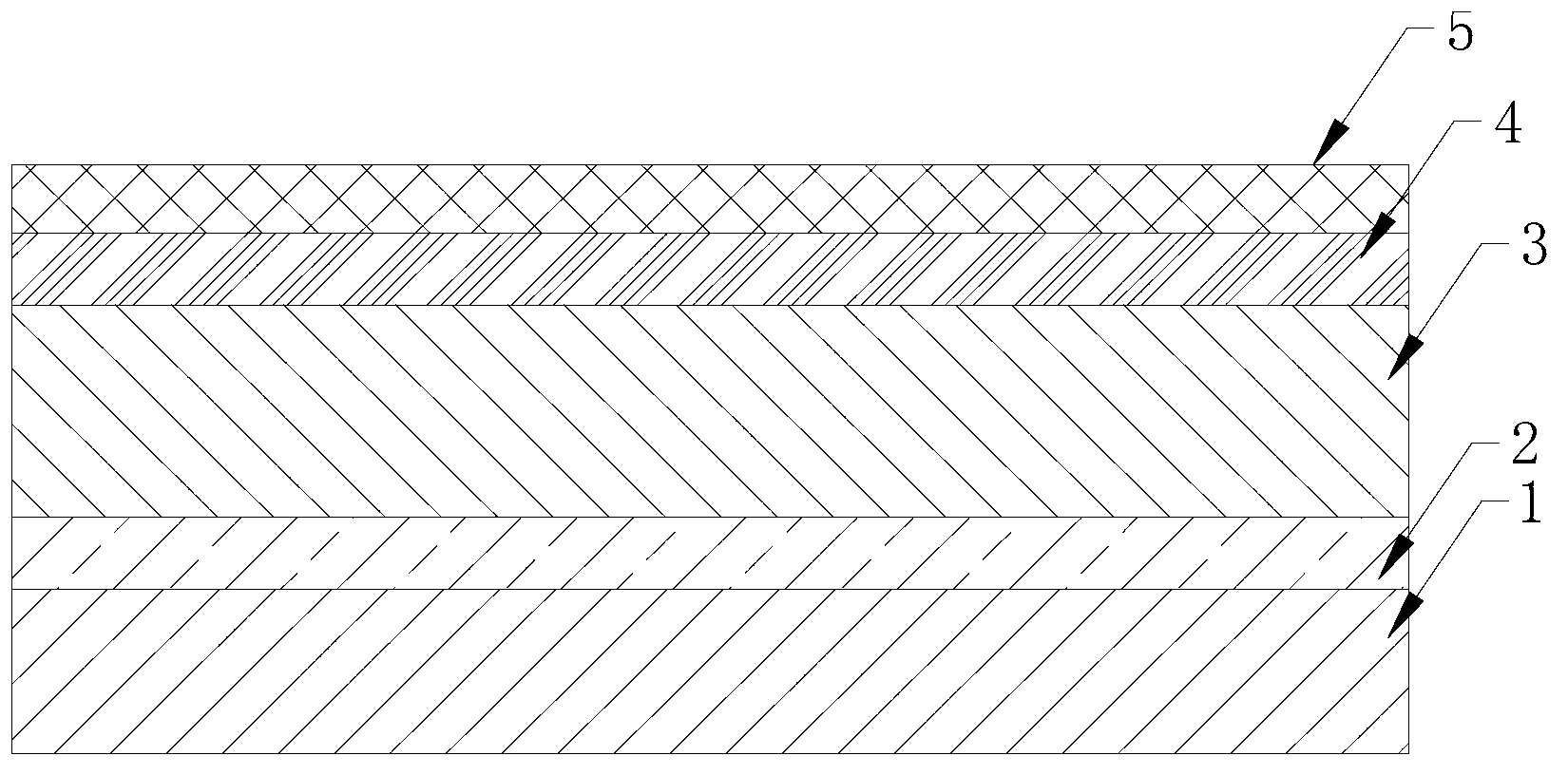
[0027] A. Provide a substrate 1; the substrate 1 is generally a III-V compound semiconductor substrate 1, such as GaAs, etc.

[0028] B. A sacrificial layer 2 is formed on the substrate 1; the sacrificial layer 2 is epitaxially grown on the substrate 1. The sacrificial layer 2 can be corroded by a specific chemical etching solution, but the chemical etching solution will not affect the active layer 3 Cause damage. The chemical etching solution here is also called stripping etching solution.

[0029] C. An active layer 3 is formed on the sacrificial layer 2; the active layer 3 is also called a device layer and is a functional layer of an electronic device.

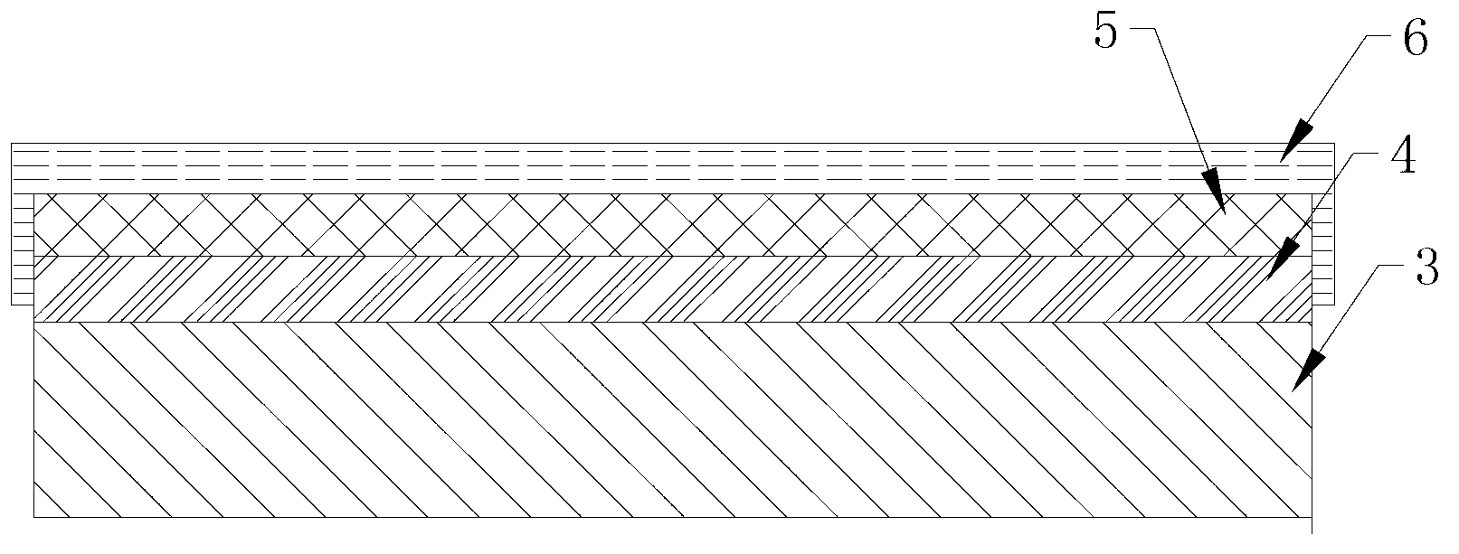
[0030] D. A backing layer is formed on the active layer 3. The backing layer includes a metal layer 4 bonded to the active layer 3 and a thermally conductive backing layer 5 adhered to the metal...

Embodiment 2

[0033] A method for preparing a III-V compound electronic device, the method comprising:

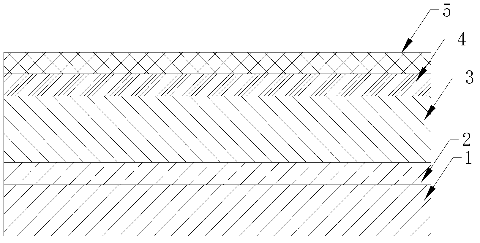
[0034] A. Provide a substrate 1; the substrate 1 is generally a III-V compound semiconductor substrate 1, such as GaAs, etc.

[0035] B. A sacrificial layer 2 is formed on the substrate 1; the sacrificial layer 2 is epitaxially grown on the substrate 1. The sacrificial layer 2 can be corroded by a specific chemical etching solution, but the chemical etching solution will not affect the active layer 3 Cause damage. The chemical etching solution here is also called stripping etching solution.

[0036] C. An active layer 3 is formed on the sacrificial layer 2; the active layer 3 is also called a device layer and is a functional layer of an electronic device.

[0037] D. Form a backing layer on the active layer 3. The backing layer includes a metal layer 4 bonded to the active layer 3 and a thermally conductive backing layer 5 adhered to the metal layer 4. When the thickness of the backing layer is...


PUM


Abstract

The invention discloses a method for preparing an III-V chemical compound electronic device. The method includes the steps that (1), a lining is provided; (2) a sacrificial layer is formed on the lining; (3) an active layer is formed on the sacrificial layer; (4) a backing layer is formed on the active layer. The backing layer comprises a metal layer adhered to the active layer and a heat-conductive backing layer pasted on the metal layer. When the thickness of the backing layer is insufficient so that the electronic device can not be supported independently, a first temporary transfer layer and a second temporary transfer layer can be utilized for transfer, and a heat-conductive supporting layer can be conveniently pasted on the heat-conductive backing layer to supply sufficient supporting force for the heat-conductive backing layer. When the thickness of the backing layer is sufficient, the electronic device can be supported independently and the backing layer is not exfoliation corrosion liquid resistant, a temporary protecting layer is pasted on the heat-conductive backing layer. After the sacrificial layer is removed through exfoliation corrosion liquid, a metal electrode is pasted on the active layer, and the temporary protecting layer is removed finally. By means of the method, the completeness of the electronic device is guaranteed, and meanwhile the electronic device of high heat dissipation performance is manufactured.

Description

Technical field [0001] The invention relates to a method for preparing a III-V compound electronic device, which belongs to the fields of high-efficiency solar energy processing, high-performance LED processing, and high-performance semiconductor physical devices. Background technique [0002] Epitaxial lift-off (ELO) technology to produce high-efficiency III-V solar cells (such as GaAs, etc.) is a relatively new technology. This technology utilizes epitaxial growth on a substrate material (generally a III-V compound semiconductor substrate, such as GaAs, etc.). Epitaxial growth includes sacrificial layer, device layer (also called active layer) and other functional layers. The sacrificial layer is etched away using a selective chemical etching solution (which can effectively etch away the sacrificial layer but does not damage the device layer), so as to realize the separation of the device layer from the substrate material. This technology mainly has the following advantages: ...

Claims


Application Information

Patent Timeline
IPC IPC(8): H01L31/18H01L31/052
CPCY02E10/50Y02P70/50
Inventor 叶继春刘凤全
Owner 苏州强明光电有限公司
Why Eureka
Try Eureka