SET/CMOS latch based on negative differential resistance characteristics

A negative differential resistor and latch technology, applied in the field of latches, can solve problems such as limiting SET output swing, increasing circuit transmission delay, and failure to obtain performance, achieving low transmission delay, high operating voltage, and low power consumption. low effect

Active Publication Date: 2013-08-21
FUZHOU UNIV
View PDF3 Cites 0 Cited by
  • Summary
  • Abstract
  • Description
  • Claims
  • Application Information

AI Technical Summary

Problems solved by technology

However, due to the disadvantages of high transmission delay and low output level of SET, the traditional circuit composed only of SET cannot obtain the required performance, and cannot be compatible with the current mature large-scale integrated circuits.
This is mainly because SET achieves current transfer through electron tunneling, which limits the size of the SET drain-source current and increases the transmission delay of the circuit; and in order to achieve Coulomb blocking, the drain-source voltage of the SET must be at a low fixed value , limits the output swing of the SET

Method used


Image

  • SET/CMOS latch based on negative differential resistance characteristics
  • SET/CMOS latch based on negative differential resistance characteristics
  • SET/CMOS latch based on negative differential resistance characteristics

Examples


Embodiment Construction

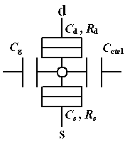
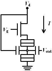
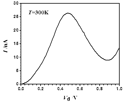
[0022] A single-electron transistor (SET) refers to a device that uses the particle and Coulomb blocking effects of electron charges to control the transfer of a single or a few electrons. Among them, the structure of a double-gate single-electron transistor is as follows figure 1 shown. The double-gate single-electron transistor is composed of two tunnel junctions connected in series through the Coulomb island, and the external bias voltage is capacitively coupled to the Coulomb island to control the tunneling current of the device; the electron tunneling is controlled by the bias voltage, The single-electron transistor has a unique Coulomb blocking oscillation characteristic, that is, as the gate voltage increases, the leakage current of the transistor has a periodic change. Unlike CMOS, single-electron transistors operate at higher drain-source voltages V ds will not enter the saturation state., with V ds The increase of the Coulomb blockage will disappear; therefore, the...


PUM


Abstract

The invention relates to an SET/CMOS latch based on negative differential resistance characteristics. The SET/CMOS latch based on the negative differential resistance characteristics comprises a double-grid single electron transistor, a PMOS tube and an NMOS tube. The SET/CMOS latch based on the negative differential resistance characteristics is characterized in that the source electrode of the PMOS tube is connected with a power source voltage Vdd, the grid electrode of the PMOS tube is used as the input end of the latch, the drain electrode of the PMOS tube is used as the output end of the latch and connected with the drain electrode of the NMOS tube and one grid electrode of the double-grid single electron transistor, the other grid electrode of the double-grid single electron transistor is connected with a control voltage Vctrl, and the source electrode of the double-grid single electron transistor is connected with the ground. Compared with a traditional CMOS latch, the latch has the advantages of being low in power consumption, simple in circuit structure, high in integration degree and the like. Compared with a single electronic latch, the latch is quite high in working voltage and large in output voltage swing, and reduces transmission delay of a circuit.

Description

technical field [0001] The invention relates to the field of latches, in particular to a SET / CMOS latch based on negative differential resistance characteristics. Background technique [0002] When the characteristic size of the MOS tube enters 100nm with the development of Moore's law, its reliability and electrical characteristics face many challenges due to the influence of quantum effects. As a new type of nanoelectronic device, single-electron transistor (single-electron transistor, SET) is expected to become a powerful substitute for MOS tubes after entering the nanometer field. SET is composed of Coulomb island, gate capacitance and two tunneling structures. It mainly controls electron tunneling through gate voltage to form current. It has ultra-small size and extremely low power consumption. In addition, single-electron transistors also have unique characteristics such as Coulomb oscillation characteristics and high charge sensitivity, which can effectively reduce t...

Claims


Application Information

Patent Timeline
Patent Type & Authority Applications(China)
IPC IPC(8): H03K19/0948
Inventor 魏榕山陈寿昌于志敏黄凤英何明华
Owner FUZHOU UNIV
Why Eureka
Try Eureka