Packaging structure for glass sealing electronic component

A technology for electronic components and packaging structures, applied in electrical components, electric solid-state devices, semiconductor devices, etc., can solve problems such as poor mechanical shock resistance, glass breakage, affecting the air tightness of the package, and achieve low loss, lead wire The effect of passing the current to increase

Active Publication Date: 2013-08-28
ZHEJIANG CHANGXING ELECTRONICS FACTORY
View PDF4 Cites 6 Cited by
  • Summary
  • Abstract
  • Description
  • Claims
  • Application Information

AI Technical Summary

Problems solved by technology

However, considering the domestic processing capacity and processing cost of such leads, the economic applicability is not high; figure 2 In the packaging form of lead wires in China, the mechanical impact resistance of the joint between the glass and the lead wire after sintering is poor, which is easy to cause glass breakage or cracks, which affects the airtightness of the package, thereby affecting the stability of electronic components.

Method used


Image

  • Packaging structure for glass sealing electronic component
  • Packaging structure for glass sealing electronic component
  • Packaging structure for glass sealing electronic component

Examples


Embodiment Construction

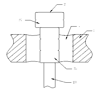
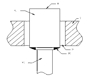
[0026] Such as figure 1 As shown, the packaging structure of the glass-encapsulated electronic components of this embodiment includes a metal substrate 7, and a sealing hole is arranged on the metal substrate 7, and a lead wire 8 is arranged in the sealing hole, and the lead wire 8 is connected to the wall of the sealing hole. Glass 9 is arranged between them, and the lead 8 includes an upper lead part 81 whose upper part is exposed on the surface of the metal substrate and the glass and passes through the sealing hole. The upper lead part 81 is a columnar structure, and the upper lead part 81 below The lower lead part 82 is connected, and the diameter of the upper lead part 81 is larger than that of the lower lead part 82; the edge of the joint between the lower lead part 82 and the upper lead part 81 is provided with a solder joint 10; in order to improve the strength and performance, The diameter of the upper lead portion 71 in this embodiment is greater than or equal to ha...


PUM


Abstract

The invention relates to an electronic component packaging structure and in particular relates to a packaging structure for a glass sealing electronic component. The packaging structure comprises a metal substrate, wherein a sealing hole is formed in the metal substrate; a lead is arranged in the sealing hole; glass is arranged between the lead and the wall of the sealing hole; the lead comprises an upper lead part of which the upper part is exposed out of the metal substrate and the surface of the glass and penetrates through the sealing hole; the upper lead part has a columnar structure; a lower lead part is connected to the lower part of the upper lead part; and the diameter of the upper lead part is larger than that of the lower lead part. According to the packaging structure for the glass sealing electronic component, the defects that the lead bonding is instable, the glass is cracked and broken, the gas tightness is low and the overall device is low in reliability in domestic similar electronic components are overcome. Compared with foreign similar electronic components, the packaging structure has the advantages that when the design is applied to a high-power packaging shell, the lead can be lower in loss by increasing the current to a certain degree.

Description

technical field [0001] The invention relates to a package structure of electronic components, in particular to a package structure of glass-sealed electronic components. Background technique [0002] When the chip is used, the chip must be isolated from the external environment to prevent impurities in the air from corroding the chip circuit and causing electrical performance degradation; on the other hand, the packaged chip is also easier to install and transport. Therefore, when a chip is used on a circuit board, it is generally necessary to package the chip. [0003] Packaging refers to connecting the circuit pins on the chip to external joints with wires so as to connect with other devices. The packaging form refers to the shell used to install the semiconductor integrated circuit chip. Protect the chip and enhance the electrothermal performance, etc., and connect the contacts on the chip to the pins of the package shell with wires, and these pins are connected to other...

Claims


Application Information

Patent Timeline
Patent Type & Authority Applications(China)
IPC IPC(8): H01L23/10H01L23/49H01L23/31
Inventor 费建超
Owner ZHEJIANG CHANGXING ELECTRONICS FACTORY
Why Eureka
Try Eureka