

Touch display device
A touch display device, a technology for displaying touch, applied in static indicators, optics, instruments, etc., can solve the problems of poor anti-interference performance, complex manufacturing process, low scanning frame rate, etc., to reduce thickness and weight, and save materials. , the effect of improving the signal-to-noise ratio
- Summary
- Abstract
- Description
- Claims
- Application Information
AI Technical Summary
Problems solved by technology
Method used
Image

Examples
Embodiment 1
[0052] Embodiment 1 of the present disclosure provides a touch display device, including:
[0053] A display touch screen, the display touch screen includes a first substrate 11, a second substrate 13, a liquid crystal layer 15 disposed between the first substrate and the second substrate, and a plurality of pixel units, the display touch screen also includes a plurality of a common electrode 17, and the plurality of common electrodes are arranged in a two-dimensional array; and
[0054] A display touch control circuit, the display touch control circuit includes a display control circuit and a touch control circuit, the display touch control circuit is connected to the plurality of common electrodes through wires in the following manner: in the display stage, the plurality of common electrodes connected to the common level provided to the display control circuit; in the touch sensing phase, each of the plurality of common electrodes is respectively connected to the touch contr...
Embodiment 2
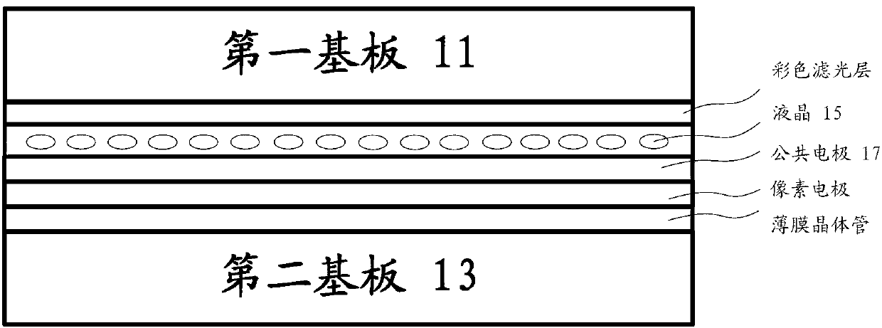
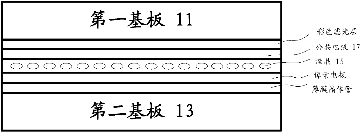
[0078] FIG. 2( a ) is a schematic side view of an example of a touch display device according to Embodiment 2 of the present disclosure.
[0079] As shown in Figure 2(a), the touch display device includes a first substrate 21, a second substrate 23, a liquid crystal layer 25 sandwiched between the two substrates, a common electrode layer 27, a thin film transistor layer and a color filter (CF )Floor. The common electrode layer is placed on the same side of the thin film transistor layer as opposed to the liquid crystal layer. Optionally, the touch display device further includes a second polarizing layer, a first polarizing layer and a protective layer (COVER LENS). As an example, the touch display device has an IPS structure. The touch display device in this embodiment may also have an FFS structure.
[0080] A plurality of pixel units are formed on the thin film transistor layer.
[0081] A plurality of common electrodes are formed on the common electrode layer, and the ...
Embodiment 3
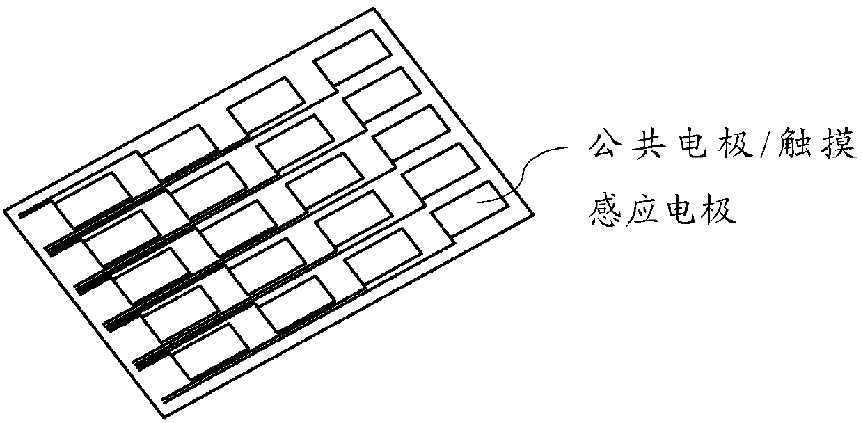
[0094] The touch display device according to this embodiment also has an IPS structure or an FFS structure. The difference between this embodiment and the second embodiment lies in the position of wire wiring. Figure 4 An example of wire wiring according to Embodiment 3 of the present disclosure is shown, and wires 501 - 503 are arranged on another layer for the common electrodes. Specifically, the wires are arranged on the same layer as the pixel electrodes, and the wires can be respectively connected to the common electrodes through through holes.
[0095] The material of the wires 501-503 can be metal oxide, such as indium tin oxide (ITO) or graphene, or metal. Preferably, the wires 501-503 are arranged directly under the black matrix. Arranging the wires under the black matrix can avoid the traces of ITO etching and the possible reflection of the metal wires.
[0096] For the description of other parts of this embodiment, please refer to Embodiment 2, which will not be...
PUM
 Abstract
Description
Claims
Application Information