Method for manufacturing a flexible electronic device using a roll-shaped motherboard, flexible electronic device, and flexible substrate
A technology of flexible electronic devices and flexible substrates, applied in semiconductor/solid-state device manufacturing, electric solid-state devices, electrical components, etc., can solve problems such as inability to use, reduce economy, weak interface adhesion, etc., achieve low cost, improve Economy, the effect of improving production speed and economy
- Summary
- Abstract
- Description
- Claims
- Application Information
AI Technical Summary
Problems solved by technology
Method used
Image

Examples
no. 1 example )
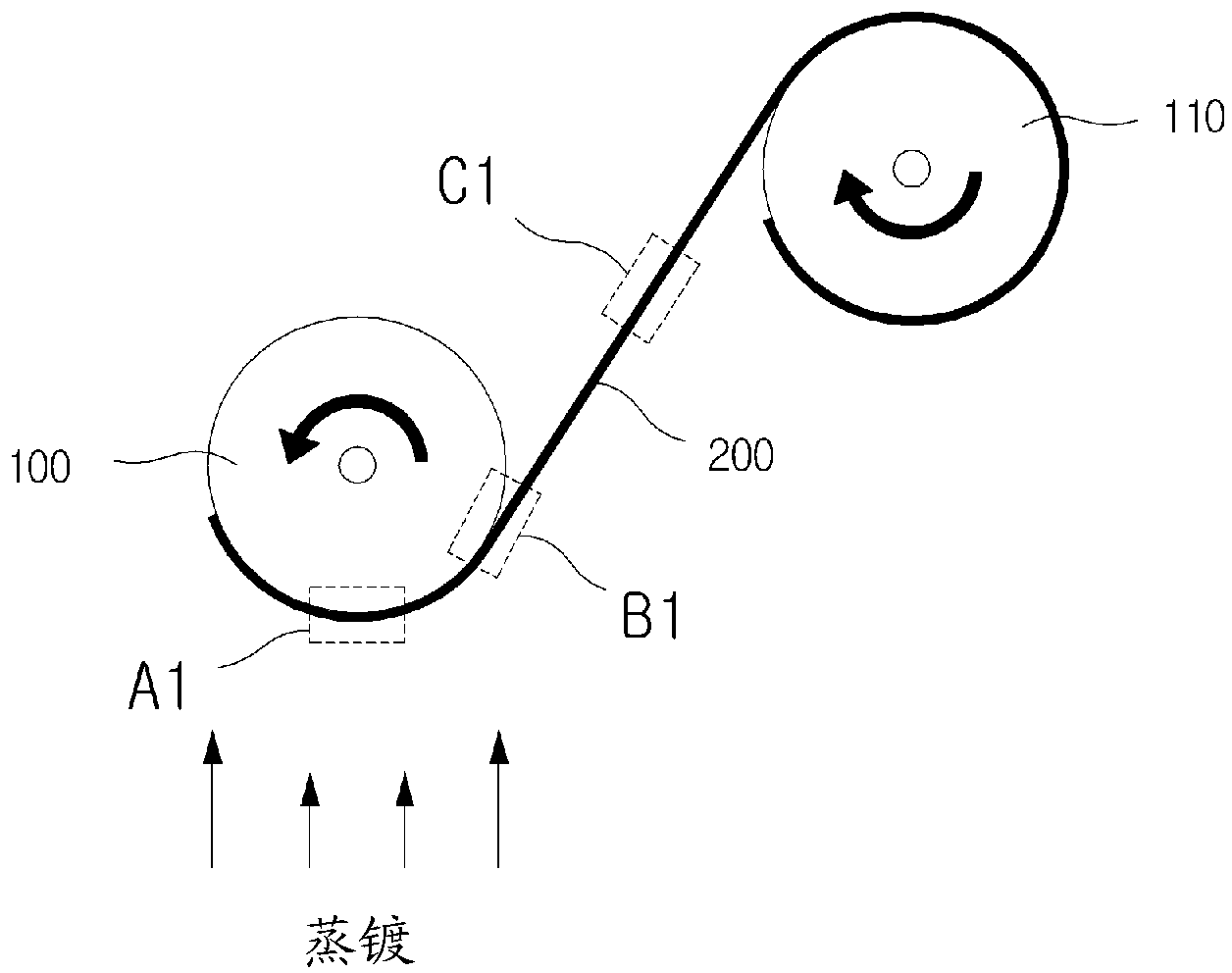
[0058] Figure 1 to Figure 5 The manufacturing method of the flexible electronic device according to the first embodiment of the present invention is schematically shown.
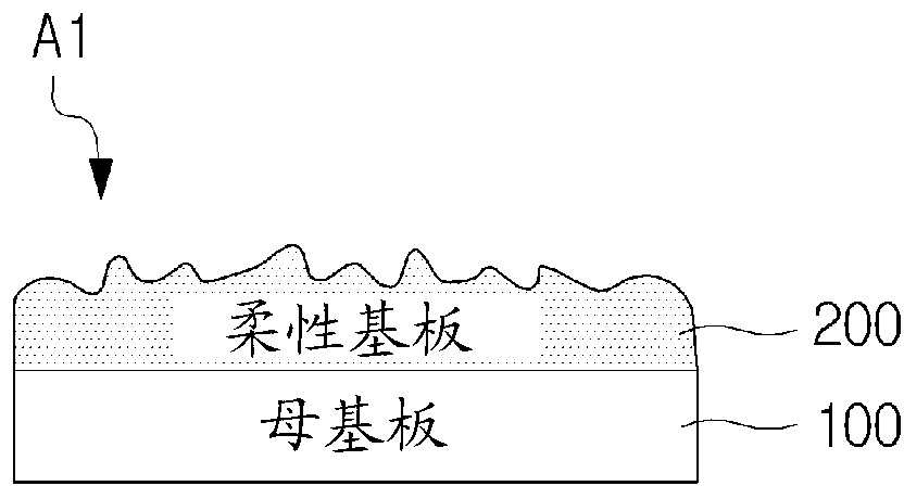
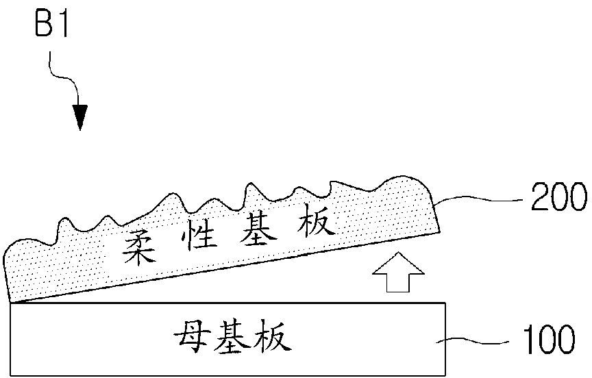
[0059] Such as Figure 1 to Figure 5 As shown, the method for manufacturing a flexible electronic device according to the first embodiment of the present invention generally includes: forming a flexible substrate 200 on a roll-shaped mother substrate 100 ( figure 1 A1 and figure 2 ), and the step of manufacturing a flexible substrate by separating the flexible substrate 200 from the roll-shaped mother substrate 100 ( figure 1 B1 and image 3 , figure 1 C1 and Figure 4 ); the step of forming the electronic device 300 and the sealing layer 400 on the separated surface of the separated flexible substrate 200 ( Figure 5 ).
[0060] In the first embodiment of the present invention, the roll-shaped mother substrate 100 uses mirror-finished surface roughness R ms p-vA stainless steel rod of <1000 nm wa...
no. 2 example )
[0063] Such as Figure 6 to Figure 8 As shown, the second embodiment of the present invention manufactures the flexible substrate 200 by a method of forming the peeling layer 500 between the roll-shaped mother substrate 100 and the flexible substrate 200 differently from the first embodiment. When the peeling layer 500 is thus formed, the separated state of the flexible substrate 200 may be: as Image 6 As shown, separated from the flexible substrate 200 interface; or as Figure 7 As shown, the interface of the roll-shaped mother substrate 100 and the release layer 500 is separated; or as Figure 8 As shown, the inner surface of the release layer 500 is separated. At this time, at Image 6 In the case of the following process may not be required, but in Figure 7 with Figure 8 In this case, an additional process of removing the peeling layer 500 is required.
[0064] Like the first embodiment of the present invention, as the separation method between the roll-shaped mot...
no. 3 example )
[0067] Figure 9 to Figure 14 A schematic representation of a method for manufacturing a flexible electronic device according to a third embodiment of the present invention.
[0068] Such as Figure 9 to Figure 14 As shown, the method for manufacturing a flexible electronic device according to the third embodiment of the present invention includes the following steps, forming a flexible substrate 200 on a roll-shaped mother substrate 100 by vapor deposition ( Figure 9 A2 and Figure 10 ) After that, the temporary substrate 600 is attached to the flexible substrate 200 by sandwiching the adhesive layer 700 thereon ( Figure 9 B2 and Figure 11 , Figure 9 C2 and Figure 12 ), and then separate the roll-shaped master substrate 100 formed on the flexible substrate 200 ( Figure 9 D2 and Figure 13 ), and then form the electronic device 300 and the sealing layer 400 on the separation surface of the flexible substrate 200, thereby manufacturing the step of the flexible elec...
PUM
| Property | Measurement | Unit |
|---|---|---|
| thickness | aaaaa | aaaaa |
| thickness | aaaaa | aaaaa |
| thickness | aaaaa | aaaaa |
Abstract
Description
Claims
Application Information
 - R&D
- Intellectual Property
- Life Sciences
- Materials
- Tech Scout
- Unparalleled Data Quality
- Higher Quality Content
- 60% Fewer Hallucinations
Browse by: Latest US Patents, China's latest patents, Technical Efficacy Thesaurus, Application Domain, Technology Topic, Popular Technical Reports.
© 2025 PatSnap. All rights reserved.Legal|Privacy policy|Modern Slavery Act Transparency Statement|Sitemap|About US| Contact US: help@patsnap.com