

Semiconductor material micro-area stress test system
A stress testing and semiconductor technology, applied in the direction of measuring the change force of optical properties of materials when they are stressed, can solve the problems of long test time and low measurement accuracy, and achieve little dependence on experience and test results. Accurate, fast and efficient test process
- Summary
- Abstract
- Description
- Claims
- Application Information
AI Technical Summary
Problems solved by technology
Method used
Image

Examples
Embodiment Construction
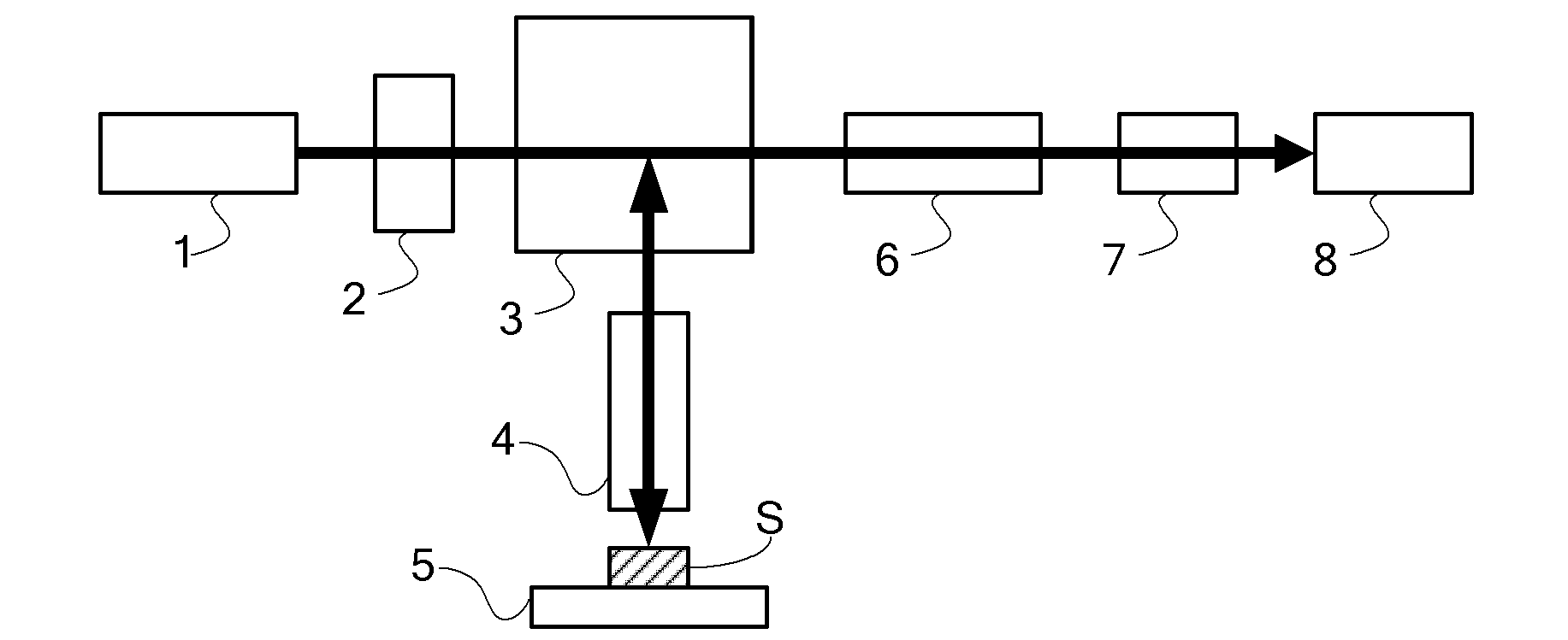
[0021] The invention proposes a brand-new micro-area stress testing system, which can perform stress testing on micron-scale areas of materials.
[0022] The principle of the micro-area testing system of the present invention is: for semiconductor materials, if there is residual stress inside, it will show anisotropy, that is, the optical axis will change. When the incident polarized laser light is reflected by the sample, the reflection coefficients of the two optical axes that exhibit anisotropy are different for the light. Residual Stress.
[0023] In order to make the object, technical solution and advantages of the present invention clearer, the present invention will be further described in detail below in conjunction with specific embodiments and with reference to the accompanying drawings.
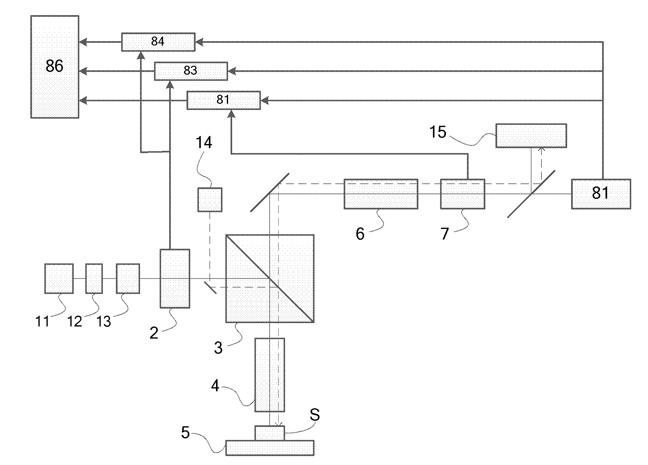
[0024] figure 1 A schematic structural diagram of the basic principle of the micro-area stress testing system of the present invention is shown. Such as figure 1 As shown, the ...
PUM
| Property | Measurement | Unit |
|---|---|---|
| pore size | aaaaa | aaaaa |
Abstract
Description
Claims
Application Information