Light-emitting diode crystal grain and manufacturing method thereof

A technology of light-emitting diodes and manufacturing methods, which is applied to semiconductor devices, electrical components, circuits, etc., can solve the problems of reducing the light-emitting efficiency of light-emitting diode crystal grains, and achieve the effect of improving light-emitting efficiency

Inactive Publication Date: 2016-07-20
ZHANJING TECH SHENZHEN +1
View PDF2 Cites 0 Cited by
  • Summary
  • Abstract
  • Description
  • Claims
  • Application Information

AI Technical Summary

Problems solved by technology

However, the above-mentioned structure has the following problems: the light emitted by the semiconductor light-emitting structure toward the substrate side will be absorbed by the substrate after entering the substrate, thereby reducing the light extraction efficiency of the light-emitting diode crystal grains

Method used


Image

  • Light-emitting diode crystal grain and manufacturing method thereof
  • Light-emitting diode crystal grain and manufacturing method thereof
  • Light-emitting diode crystal grain and manufacturing method thereof

Examples


Embodiment Construction

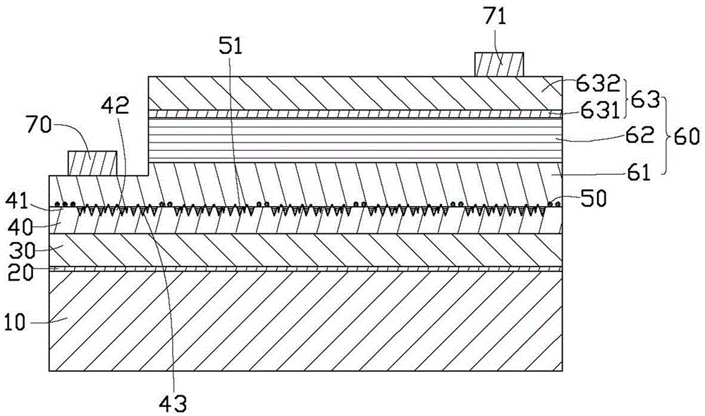
[0020] Such as figure 1 As shown, the LED die 100 provided in the first embodiment of the present invention includes: a substrate 10, a buffer layer 20 formed on the substrate 10, a transition layer formed on the buffer layer 20, and a buffer layer formed on the buffer layer 20. Aluminum nitride 50 on the transition layer, and an electrical layer 60 formed on the transition layer and covering the aluminum nitride 50 .

[0021] The substrate 10 is in the shape of a regular flat plate, which can be made of materials such as sapphire, silicon carbide (SiC), silicon (Si) or gallium nitride (GaN), preferably sapphire in this embodiment, to control light emission Chip manufacturing costs.

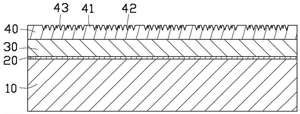
[0022] The transition layer includes a first transition layer 30 and a second transition layer 40 formed on the first transition layer 30 . The buffer layer 20, the first transition layer 30 and the second transition layer 40 can be deposited by metal-organic chemical vapor deposition (Metal-Or...


PUM


Abstract

A kind of glowing diode grain, including the substrate and an electrical layer formed on the substrate, forming a transition layer between the substrate and the electrical layer, which includes the flat -scale flat area and rough pattern area of the surface.The surface of the flat area of the transition layer is contacted and the electrical layer and the transition layer are clamped with spherical aluminum nitride, and the gap between the electrical layer and the pattern area of the transition layer.The invention first forms a rough surface between the electrical layer and the substrate, and then forms a spherical aluminum nitride between the transition layer and the electrical layer.A gap between the formation can increase the probability of the light of the light from the factor plate emitted by the lighting layer through the full reflection, thereby improving the lighting efficiency of the luminous diode grain.The present invention also involves a manufacturing method of the glowing diodes.

Description

technical field [0001] The invention relates to a light-emitting diode crystal grain and a manufacturing method thereof, in particular to a light-emitting diode crystal grain with high light extraction efficiency and a manufacturing method thereof. Background technique [0002] A light emitting diode (Light Emitting Diode, LED) is a semiconductor element that can convert current into light in a specific wavelength range. Light-emitting diodes can be widely used as light sources in the field of lighting because of their advantages such as high brightness, low operating voltage, low power consumption, easy matching with integrated circuits, simple driving, and long life. [0003] Existing light-emitting diode grains generally include a substrate and a semiconductor light-emitting structure grown on the surface of the substrate. However, the above structure has the following problem: the light emitted by the semiconductor light-emitting structure towards the substrate will be ...

Claims


Application Information

Patent Timeline
Patent Type & Authority Patents(China)
IPC IPC(8): H01L33/10H01L33/22
CPCH01L33/10H01L33/22H01L33/32H01L33/58
Inventor 黄嘉宏黄世晟凃博闵林雅雯杨顺贵
Owner ZHANJING TECH SHENZHEN
Why Eureka
Try Eureka