Unlock instant, AI-driven research and patent intelligence for your innovation.

A packaging structure and packaging method for a high-power linear array laser

A line array laser and packaging structure technology, applied in the direction of lasers, laser components, semiconductor lasers, etc., can solve problems such as inability to ensure strict collinearity, low reliability of series circuits, and unguaranteed level of light output, etc., to increase work Stability, improved heat dissipation, and high reliability

Active Publication Date: 2015-08-19
Shandong Huaguang Optoelectronics Co. Ltd.
View PDF8 Cites 0 Cited by
  • Summary
  • Abstract
  • Description
  • Claims
  • Application Information

AI Technical Summary

Problems solved by technology

However, in the existing scheme, each single tube cannot ensure strict collinearity, and the level of light output cannot be guaranteed, and the reliability of the series circuit formed by welding each single tube with gold wire is not high.

Method used


Image

  • A packaging structure and packaging method for a high-power linear array laser
  • A packaging structure and packaging method for a high-power linear array laser
  • A packaging structure and packaging method for a high-power linear array laser

Examples


Embodiment 1

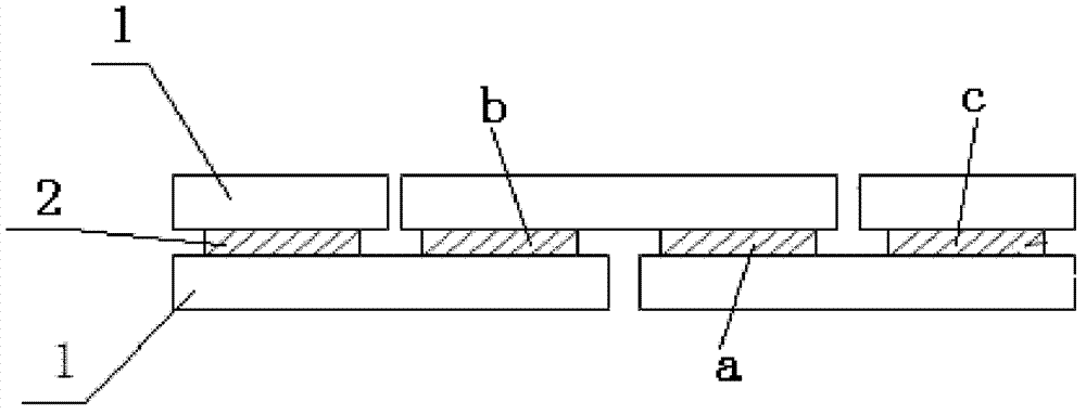
[0032] Such as Figure 1-3 As shown, a packaging structure of a high-power line array laser includes a plurality of semiconductor bar line array lasers 2 arranged at equal intervals in a straight line, and two adjacent semiconductor bar bar line array lasers 2 are arranged in reverse, for example : The p-side electrode of a semiconductor bar line array laser faces up, and the n-side electrode faces down; the p-side electrode of the adjacent semiconductor bar line array laser faces down, and the n-side electrode faces up, that is, the electrode direction is opposite;

[0033] The p-face electrode of the semiconductor bar line array laser a is connected in series with the n-face electrode of the semiconductor bar line array laser b adjacent to one side through the heat sink 1, and the n-face electrode of the semiconductor bar line array laser a The p-plane electrodes of the semiconductor bar line array laser c adjacent to the other side are connected in series through the heat s...

Embodiment 2

[0039] A packaging method for packaging structure as described in embodiment 1, comprising steps as follows:

[0040] (1) According to the prior art, a plurality of semiconductor bar line array lasers 2 are welded and arranged in the insulating region 5 of the insulating ceramic substrate 10 according to straight lines; one side of the insulating ceramic substrate 10 is provided with a patterned metal layer 4, The pattern shape of the pattern metal layer is adapted to the arrangement shape of the heat sink 1; the two adjacent semiconductor bar line array lasers 2 are set in reverse; the area outside the pattern metal layer 4 is an insulating area 5 .

[0041] (2) The p-face electrode of the semiconductor bar line array laser a is connected in series with the n-face electrode of the semiconductor bar line array laser b adjacent to one side through the heat sink 1, and the semiconductor bar bar line array laser a is connected in series. The n-face electrode is connected in seri...


PUM


Abstract

The invention relates to a packaging structure of a large-power linear array laser device. The packaging structure comprises a plurality of semiconductor bar linear array laser devices which are arrayed on the same straight line at equal intervals, wherein the two adjacent semiconductor bar linear array laser devices are arranged oppositely; a p-face electrode of each semiconductor bar linear array laser device is connected with an n-face electrode of the semiconductor bar linear array laser device at the adjacent side through a heat sink in series; the n-face electrode of the semiconductor bar linear array laser device is connected with a p-face electrode of the semiconductor bar linear array laser device at the other adjacent side through a heat sink in series; and the semiconductor bar linear array laser devices located at the two ends of the packaging structure of the large-power linear array laser device are connected with an external power supply through heat sinks to form a series circuit. According to the packaging structure disclosed by the invention, the two adjacent semiconductor bar linear array laser devices are welded on one heat sink to realize parallelism of a slow axis of a pumping source output light beam and an axis of a YAG (Yttrium Aluminum Garnet) laser rod of a side pump; and the problem that linear array pumping source output light beams are not collinear is effectively avoided so that the light output conversion efficiency is improved.

Description

technical field [0001] The invention relates to a packaging structure and a packaging method of a high-power linear array laser, belonging to the technical field of laser packaging. Background technique [0002] The all-solid-state laser pumped by semiconductor laser is a new type of laser that appeared in the late 1980s. Its overall efficiency is at least 10 times higher than that of lamp pumping. Due to the reduced heat load per unit output, higher power can be obtained, and the system life and reliability are about 100 times that of flash lamp pumping systems. Therefore, semiconductor laser pumping technology It injects new vitality and vitality into solid-state lasers, so that all-solid-state lasers have the dual characteristics of solid-state lasers and semiconductor lasers. Its appearance and gradual maturity are a revolution of solid-state lasers and the development direction of solid-state lasers. Moreover, it has penetrated into various disciplines, such as: laser ...

Claims


Application Information

Patent Timeline
Patent Type & Authority Patents(China)
IPC IPC(8): H01S5/024
Inventor 张骋王娜李沛旭汤庆敏
Owner Shandong Huaguang Optoelectronics Co. Ltd.