Supercharge Your Innovation With Domain-Expert AI Agents!

Analog switch control circuit structure

An analog switch and control circuit technology, applied in the field of switch control circuit and semiconductor integrated circuit design, can solve the problem that the transmission gate cannot be closed, and achieve the effects of stable and reliable working performance, simple and practical structure, and a wide range of applications

Active Publication Date: 2013-09-18
CRM ICBG (WUXI) CO LTD
View PDF4 Cites 24 Cited by
  • Summary
  • Abstract
  • Description
  • Claims
  • Application Information

AI Technical Summary

Problems solved by technology

[0009] The problem with this circuit is that this switch cannot be used to transmit negative level signals, because when the input signal IN voltage is lower than -VDN, the N1 parasitic diode conducts forward, forming a leakage current from IN to GND; when the input signal IN voltage is lower than -VDN When -|VTN| is lower than -VDN, |VGSN| of N1>|VTN|, N1 is turned on, there is a path between IN and OUT, and the parasitic diode of N1 is forward-conducting, so there is a leakage current from IN, OUT to GND
[0010] In addition, when the VDD voltage drops to equal to the ground, if there is still an input signal at the IN terminal, the transmission gate cannot be closed

Method used


Image

  • Analog switch control circuit structure
  • Analog switch control circuit structure

Examples


Embodiment Construction

[0021]In order to understand the technical content of the present invention more clearly, the following embodiments are given for detailed description.

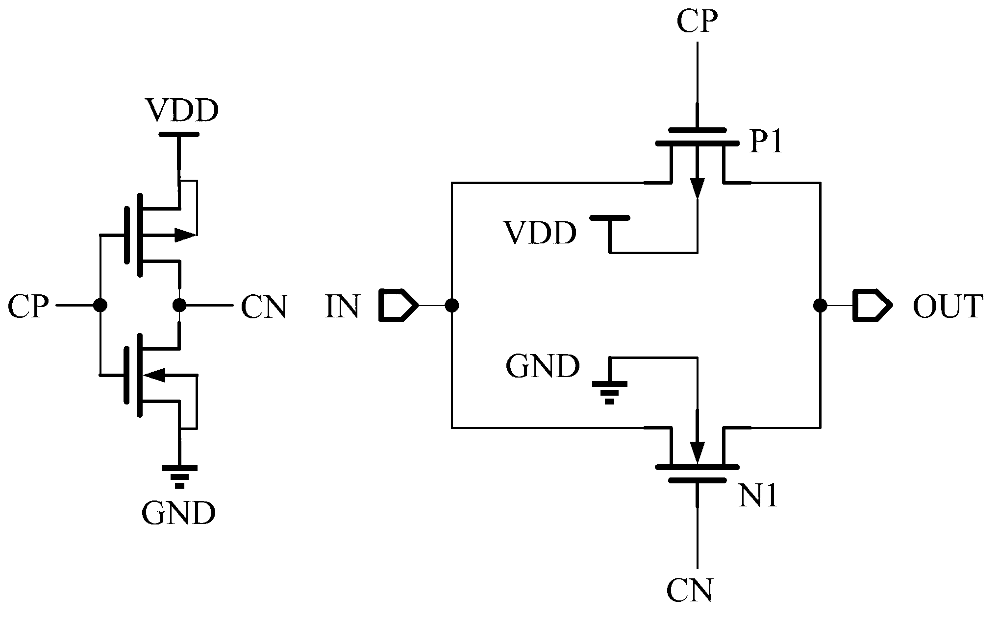
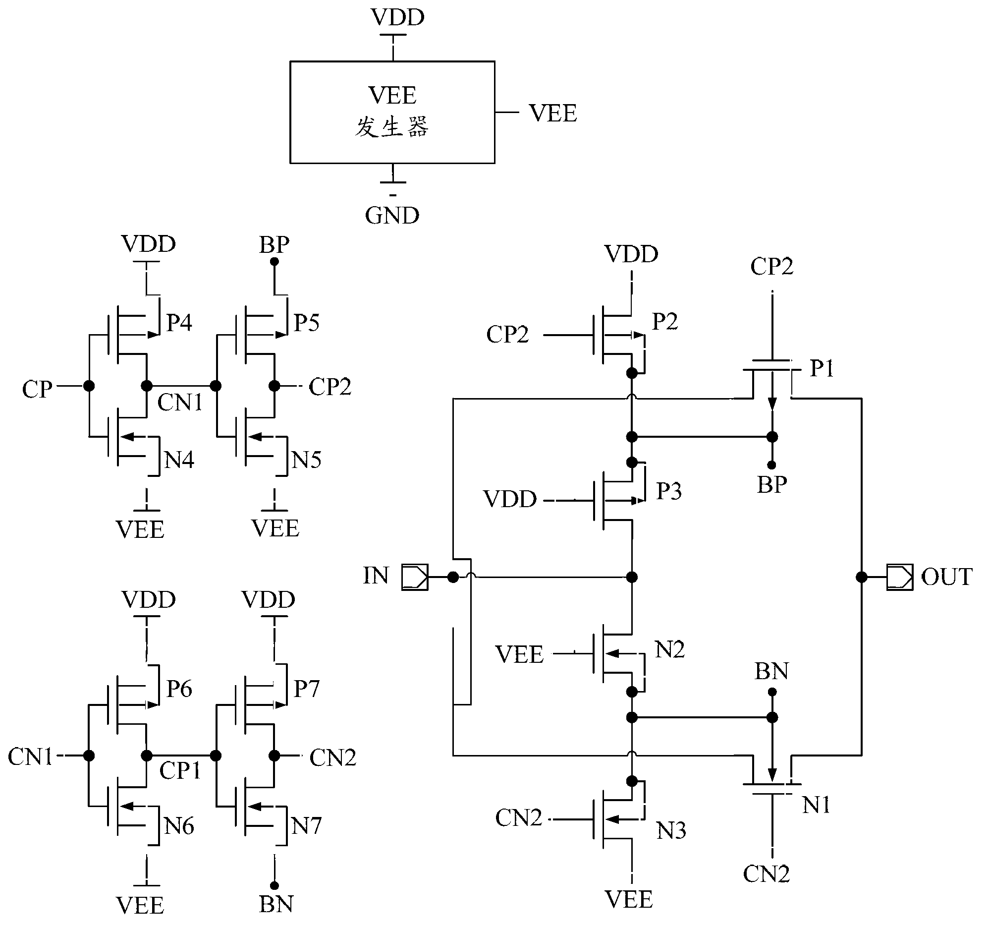
[0022] see figure 2 As shown, the analog switch control circuit structure includes a transmission gate PMOS field effect transistor P1, a transmission gate NMOS field effect transistor N1, a negative voltage generating circuit module, a first inverter circuit module, a second inverter circuit module, The PMOS substrate gate control circuit module and the NMOS substrate gate control circuit module, the source of the transmission gate PMOS field effect transistor P1 and the source of the transmission gate NMOS field effect transistor N1 are both connected to the analog signal input end , the drain of the transmission gate PMOS field effect transistor P1 and the drain of the transmission gate NMOS field effect transistor N1 are both connected to the analog signal output end, and the substrate and the gate of the transmission ga...


PUM


Abstract

The invention relates to an analog switch control circuit structure, which is characterized by comprising a transmission gate PMOS (P-channel Metal Oxide Semiconductor) field effect transistor (P1), a transmission gate NMOS (N-channel Metal Oxide Semiconductor) field effect transistor (N1), a negative voltage generation circuit module, a first inverter circuit module, a second inverter circuit module, a PMOS substrate gate control circuit module and an NMOS substrate gate control circuit module. By using the analog switch control circuit structure, a negative level signal can be transmitted, the gate potentials of the PMOS transistor and the NMOS transistor in a transmission gate can be controlled, the PMOS transistor and the NMOS transistor are turned off during power failure, all input signals cannot be transmitted to an output end under the condition that the input signal is of positive level or negative level, and the parasitic diodes of the PMOS transistor and the NMOS transistor are controlled to be not connected through the transmission gate substrate potential control circuit; the PMOS transistor and the NMOS transistor are not turned on through the gate potential control circuit during power failure; and the analog switch control circuit structure has the advantages of simple and practical structure, stable and reliable working performance and wider application range.

Description

technical field [0001] The invention relates to the field of semiconductor integrated circuit design, in particular to the technical field of switch control circuits, in particular to an analog switch control circuit structure. Background technique [0002] Nowadays, various analog circuits need analog transmission switches to transmit and select analog input signals. For example, audio and video circuits require transmission switches to select and turn on audio and video signals, and analog control circuits require transmission switches to control signals. selection control. Various transmission circuits place higher and higher demands on the performance of analog switches. [0003] The traditional analog switch circuit uses the transmission gate as the transmission switch, the transmission gate adopts the parallel connection mode of PMOS and NMOS, the substrate of PMOS is connected to the power supply of the circuit, and the substrate of NMOS is connected to the ground of...

Claims


Application Information

Patent Timeline
Patent Type & Authority Applications(China)
IPC IPC(8): H03K17/687
Inventor 夏虎徐栋严淼罗先才朱立群张蓉
Owner CRM ICBG (WUXI) CO LTD
Features
  • R&D
  • Intellectual Property
  • Life Sciences
  • Materials
  • Tech Scout
  • Unparalleled Data Quality
  • Higher Quality Content
  • 60% Fewer Hallucinations
Learn More