Single event upset resisting reinforcing system and method used for FPGA (Field Programmable Gate Array)

An anti-single event and reloading technology, applied in the direction of information storage, static memory, digital memory information, etc., can solve the problems of not being able to meet different needs, single interface mode, lack of portability, etc., to achieve enhanced applicability, The effect of enhancing operability

Active Publication Date: 2013-09-25
SHANGHAI SPACEFLIGHT INST OF TT&C & TELECOMM
View PDF5 Cites 23 Cited by
  • Summary
  • Abstract
  • Description
  • Claims
  • Application Information

AI Technical Summary

Problems solved by technology

[0009] The main disadvantage of the above method to improve the anti-single event upset of FPGA devices is that although the cumulative effect of FPGA single event upsets can be completely eliminated through the readback reload operation, it causes the functional interruption of the FPGA device and is only used for its own model of FPGA. not portable
At the same time, the interface mode is also fixed as JTAG, which is not applicable to the model tasks using the SelectMAP interface
[0010] To sum up, using the existing anti-single event effect hardening method requires a large number of design modifications for different types of FPGA devices, which is not universal; and the interface method is single, which cannot meet different needs

Method used


Image

  • Single event upset resisting reinforcing system and method used for FPGA (Field Programmable Gate Array)
  • Single event upset resisting reinforcing system and method used for FPGA (Field Programmable Gate Array)
  • Single event upset resisting reinforcing system and method used for FPGA (Field Programmable Gate Array)

Examples


Embodiment

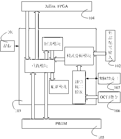
[0059] Such as figure 1 Shown is an embodiment of the present invention, and host computer is connected with communication interface module by serial port 107; The dedicated pin of Xilinx SRAM type FPGA 104 that the user selects is connected with readback refresh control device 103 according to different interface modes; Store FPGA configuration file The PROM 105 is also connected to the reload module, the readback module and the refresh module respectively according to different interface modes.

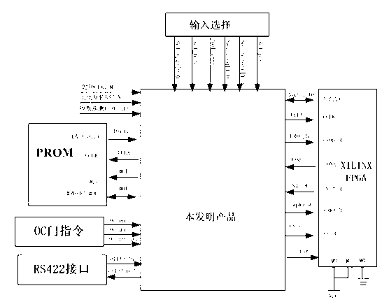
[0060] According to the external configuration 102 selected by the user, the FPGA device model, interface mode, readback refresh mode, power-on ban, readback cycle and readback overload threshold are determined. image 3 and Figure 4 Corresponding to the input selection signals Sel_fpga[2:0], Sel_intf, Sel_mode, Sel_per, Sel_freq[1:0], Sel_biterr[1:0], the operations corresponding to different values ​​are shown in the table below.

[0061] Sel_fpga[2:0] is used to select the FPG...


PUM


Abstract

The invention provides a single event upset resisting reinforcing system used for an FPGA (Field Programmable Gate Array). The single event upset resisting reinforcing system comprises a clock pulse source, a backward read refresh controller, an external configuration input unit, an FPGA, a PROM (Programmable Read Only Memory) and an external communication interface, wherein the clock pulse source, the external configuration input unit, the FPGA, the PROM and the external communication interface are respectively connected with the backward read refresh controller; the clock pulse source provides a clock pulse for the backward read refresh controller; the external configuration input unit is used for configuring initial data of the system through inputting a selection signal; original configuration data of the FPGA is stored in the PROM; the backward read refresh controller is used for loading, backwards reading and refreshing the configuration data of the FPGA; the external communication interface is an interface for sending a remote control command to the system and receiving a telemetering command of the system, which is provided for a user.

Description

technical field [0001] The invention belongs to the technical field of strengthening the anti-single event effect capability of semiconductor devices, and in particular relates to an anti-single event inversion strengthening system for FPGA and a method thereof. Background technique [0002] SRAM-based FPGA devices have the characteristics of rich logic resources, more internal available RAM, convenient programming, and reconfigurability. FPGA division of choice. However, the FPGA based on SRAM technology is greatly affected by high-energy particles in space, and the logic state of its internal configuration memory is often flipped due to particle impact, that is, single event upset (SEU). If the flipping occurs in the logic function area, it may cause the function interruption of the spacecraft; if the flipping occurs in the RAM unit, it may cause data error or loss, which cannot meet the requirements of high-reliability products such as satellites. Aerospace products nee...

Claims


Application Information

Patent Timeline
Patent Type & Authority Applications(China)
IPC IPC(8): G11C11/413G11C29/00
Inventor 王琰朱新忠魏文超冯书谊
Owner SHANGHAI SPACEFLIGHT INST OF TT&C & TELECOMM
Why Eureka
Try Eureka