Fin field effect transistor and technology thereof

A technology of field-effect transistors and transistors, which is applied in semiconductor devices, semiconductor/solid-state device manufacturing, electrical components, etc., and can solve problems such as reduced component performance, increased gate dielectric layer thickness, and decreased gate capacitance

Inactive Publication Date: 2013-09-25
UNITED MICROELECTRONICS CORP
View PDF4 Cites 9 Cited by
  • Summary
  • Abstract
  • Description
  • Claims
  • Application Information

AI Technical Summary

Problems solved by technology

However, as the size of MOS transistors continues to shrink, traditional polysilicon gates have lower device performance due to boron penetration (boron penetration) effect, and the unavoidable depletion effect (depletion effec

Method used


Image

  • Fin field effect transistor and technology thereof
  • Fin field effect transistor and technology thereof
  • Fin field effect transistor and technology thereof

Examples


Embodiment Construction

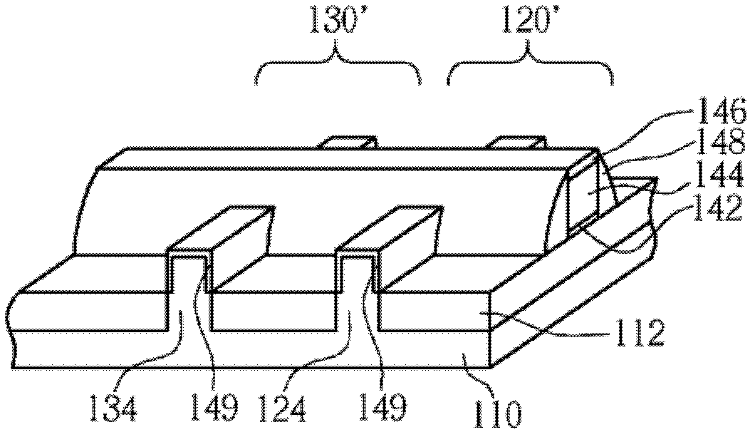
[0024] Figure 1-2 A three-dimensional view of a fin field effect transistor process according to an embodiment of the present invention is shown. Such as figure 1 As shown, first, a substrate 110 is provided. Then, the first FinFET 120' and the second FinFET 130' are formed on the substrate 110.

[0025] In detail, the method for forming the first FinFET 120' and the second FinFET 130' may include: providing a bulk substrate (not shown), forming a hard mask layer (not shown) thereon ), and pattern it to define the first fin structure 124 and the second fin field effect transistor 130' corresponding to the first fin field effect transistor 120' to be formed in the underlying bulk substrate The second fin structure 134 is located at the base 110 . Next, an etching process is performed to simultaneously form the first fin structure 124 and the second fin structure 134 on the substrate 110 in a bulk substrate (not shown). In this way, the fabrication of the first fin structu...


PUM


Abstract

The invention discloses a fin field effect transistor and the technology of the fin field effect transistor. The technology of the fin field effect transistor comprises the following steps that a substrate is provided; a first fin field effect transistor and a second field effect transistor are formed on the substrate, wherein the first fin field effect transistor comprises a first metal layer, and the second fin field effect transistor comprises a second metal layer; the processing technology is conducted on the first metal layer to change the threshold voltage of the first fin field effect transistor.

Description

technical field [0001] The present invention relates to a fin field effect transistor (FinFET) and its process, and in particular to a fin field effect transistor (FinFET) and its process, which changes the physical properties of the metal layer in the field effect transistor by performing a treatment process properties or chemical properties. Background technique [0002] In the known semiconductor industry, polysilicon is widely used in semiconductor devices such as metal-oxide-semiconductor (MOS) transistors as a standard gate filling material of choice. However, as the size of MOS transistors continues to shrink, traditional polysilicon gates have lower device performance due to boron penetration (boron penetration) effect, and the unavoidable depletion effect (depletion effect) and other problems, so that the equivalent gate The thickness of the dielectric layer increases and the capacitance value of the gate decreases, which leads to the decline of the driving ability...

Claims


Application Information

Patent Timeline
IPC IPC(8): H01L21/336H01L29/78
Inventor 林建廷江文泰
Owner UNITED MICROELECTRONICS CORP
Why Eureka
Try Eureka