Enhanced silicon-based photodiode and method of making the same

A photodiode, enhanced technology, applied in circuits, electrical components, semiconductor devices, etc., can solve the problems of background noise interference, poor UV selectivity, and high error rate, and achieve a reduction in the degree of response, quantum efficiency and response rate improvement. The effect of UV selectivity

Active Publication Date: 2015-10-07
SHENZHEN AIXIESHENG TECH CO LTD
View PDF3 Cites 2 Cited by
  • Summary
  • Abstract
  • Description
  • Claims
  • Application Information

AI Technical Summary

Problems solved by technology

[0004] However, since silicon materials have a very shallow absorption depth for ultraviolet / blue-violet light, the main reason is that the absorption coefficient of ultraviolet / blue-violet light in silicon materials is very large, and almost all light waves with wavelengths less than 380nm are absorbed within a depth of 100nm from the silicon surface. Completely absorbed, the UV photodiodes made under the traditional standard CMOS process show a strong response to visible light / near-infrared light. From a certain point of view, their UV selectivity is very poor, and the background noise interferes a lot. In the UV flame High error rate in detection, UV alarm and other applications

Method used


Image

  • Enhanced silicon-based photodiode and method of making the same
  • Enhanced silicon-based photodiode and method of making the same
  • Enhanced silicon-based photodiode and method of making the same

Examples


Embodiment Construction

[0066] The following will clearly and completely describe the technical solutions in the embodiments of the present invention with reference to the accompanying drawings in the embodiments of the present invention. Obviously, the described embodiments are only part of the embodiments of the present invention, not all of them. Based on the embodiments of the present invention, all other embodiments obtained by persons of ordinary skill in the art without creative efforts fall within the protection scope of the present invention.

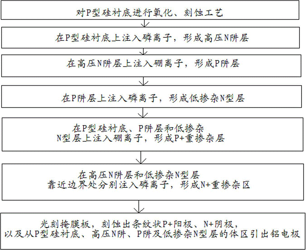
[0067] The embodiment of the invention discloses an enhanced silicon-based photodiode and a manufacturing method thereof, so as to realize that the ultraviolet photodiode has a simple structure, is easy to manufacture, and has the advantages of high ultraviolet selectivity, high ultraviolet responsivity, and low response time.

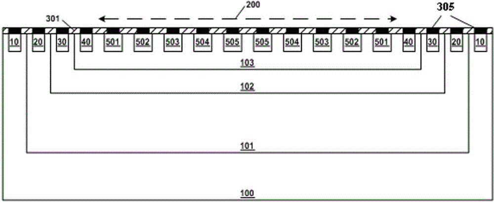
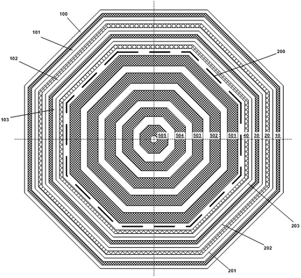
[0068] Such as figure 1 Shown, an enhanced silicon-based photodiode, including:

[0069] P-type silicon substrate 100;

[...


PUM


Abstract

The invention discloses an enhanced type silicon-based photodiode and a manufacturing method thereof. The photodiode comprises a P-type substrate, wherein a high-voltage deep N well is arranged on the P-type substrate; a P well is arranged on the high-voltage deep N well; a stripe-shaped p<+> anode is injected on a low doped N layer; and the stripe-shaped P<+> anode and the low doped N layer form a photodiode structure with ultraviolet / blue-violet enhanced response. The low-doped N type layer and the P well form a parasitic photodiode; the P well and the high-voltage N well form a parasitic diode; the two electrodes form a back-to-back structure; a short circuit structure is formed at an electrode lead-out end, so that the response degree of the enhanced type silicon-based photodiode on visible / near-infrared light can be effectively isolated and lowered, and ultraviolet selectivity of the enhanced type silicon-based photodiode is greatly improved. The layout of the enhanced type silicon-based photodiode is designed into an octagonal ring-shaped structure, so that an edge breakdown effect is effectively lowered. A photosensitive window is designed into a ring-shaped stripe structure, so that the ultraviolet response degree and the quantum efficiency are improved, and the response time is shortened.

Description

technical field [0001] The invention relates to a silicon-based photodiode, more specifically, to a silicon-based photodiode with greatly enhanced ultraviolet selectivity and ultraviolet responsivity and a manufacturing method thereof. Background technique [0002] At present, with the rapid development of microelectronics technology and integrated circuit technology, the performance of ultraviolet photodiodes has been significantly improved in terms of responsivity, quantum efficiency, and integration. At present, there are mainly three types of ultraviolet photodiodes: photoemissive ultraviolet photodiodes, wide-bandgap semiconductor ultraviolet photodiodes, and silicon-based PN junction ultraviolet photodiodes. Photoemissive UV photodiodes are expensive, bulky and fragile, they are prone to fatigue and aging, making them less sensitive, they must avoid high-intensity radiation, store in a dark place, and require high reverse bias voltage, so the application is limited. ...

Claims


Application Information

Patent Timeline
Patent Type & Authority Patents(China)
IPC IPC(8): H01L31/102H01L31/0352H01L31/18
Inventor 金湘亮陈长平
Owner SHENZHEN AIXIESHENG TECH CO LTD
Why Eureka
Try Eureka