Semiconductor device
A semiconductor and device technology, applied in the field of n-type semiconductor semiconductor devices and semiconductor devices, can solve problems such as leakage current, affecting the stability and reliability of semiconductor devices, and affecting luminous efficiency, so as to improve efficiency and reliability, and luminous Optimum effect on area and light output
- Summary
- Abstract
- Description
- Claims
- Application Information
AI Technical Summary
Problems solved by technology
Method used
Image

Examples
Embodiment 1
[0025] The semiconductor device of the present invention includes a substrate having an n-type semiconductor provided with an n-type electrode and a semiconductor chip including a p-type semiconductor provided with a p-type electrode on the substrate, and one of the epitaxial crystal layers exposed on the side of the semiconductor chip The junction between the two is covered with an insulating layer. The insulating layer prevents conduction and leakage between the epitaxial crystal layers. Taking optoelectronic semiconductor as an example, the details of optoelectronic semiconductor device are as follows:
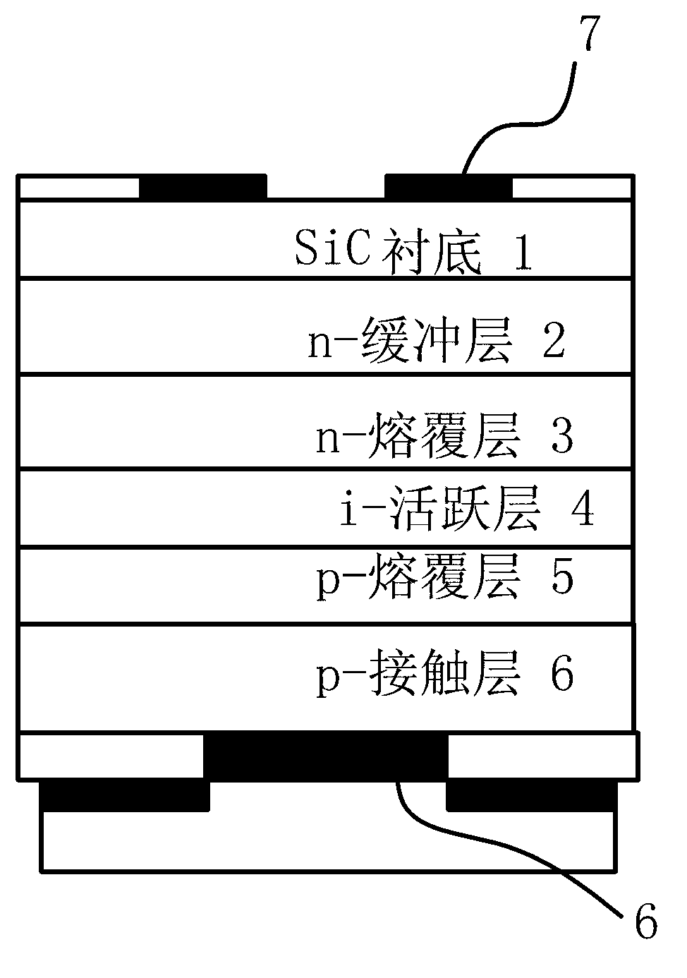
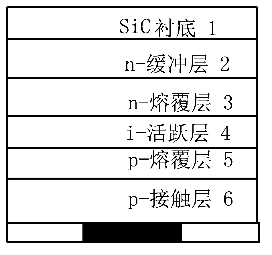
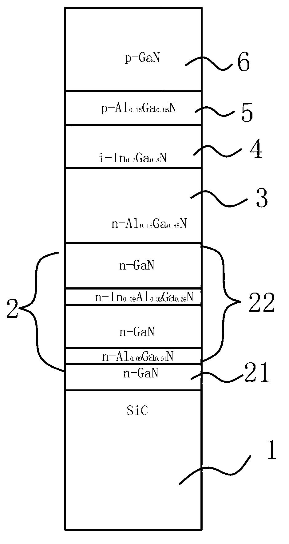
[0026] Such as figure 1 with figure 2 The optoelectronic semiconductor device shown includes a substrate 1, a buffer layer 2 on the substrate 1, and an n-type contact layer 7 on the other side of the substrate 1, and an n-type cladding layer 3 on the buffer layer 2. The light-emitting layer 4, the p-type cladding layer 5 and the p-type contact layer 6, the p-type contact lay...
Embodiment 2
[0035] The second embodiment is basically the same as the first embodiment. The difference is that when the production of the semiconductor device is started after the fabrication of the optoelectronic semiconductor epitaxial crystal sheet, the epitaxial crystal sheet is first physically cut, and then the epitaxial crystal sheet is etched to make each layer section of the epitaxial crystal sheet Level, and then cover the junction between the epitaxial crystal layers exposed on the side of the semiconductor chip with an insulating layer 8 made of plastic or resin; then make a p-type electrode on the p-type contact layer of the epitaxial layer, and then apply it to the electronic semiconductor An n-type electrode is made on the n-type contact layer on the back of the epitaxial crystal sheet, and then the optoelectronic semiconductor epitaxial crystal sheet is cut or broken to form a semiconductor chip. Physical cutting of the epitaxial crystal sheet will cause dislocation and unev...
Embodiment 3
[0037] Such as Figure 5 As shown, the semiconductor device includes a substrate, a semiconductor chip of an n-type semiconductor with an n-type electrode and a p-type semiconductor with a p-type electrode on the substrate, and one of two or more adjacent light-emitting areas in the semiconductor chip A non-conductive insulating separation layer 9 is formed therebetween. The insulating separation layer 9 is formed by an ion implantation method or a doping method or by etching a trench and filling an insulating material. details as follows:
[0038] Use photolithography to attach a protective film to prevent ion implantation on the surface of the wafers in two or more adjacent light-emitting areas, and then open the window of the chip pattern on the protective film, and then use B ions or O 2 Ions are injected between adjacent light-emitting areas under an acceleration voltage of 100KV to form an insulating separation layer 9, that is, an insulating layer. Other content can be c...
PUM
| Property | Measurement | Unit |
|---|---|---|
| Roughness | aaaaa | aaaaa |
Abstract
Description
Claims
Application Information
 - Generate Ideas
- Intellectual Property
- Life Sciences
- Materials
- Tech Scout
- Unparalleled Data Quality
- Higher Quality Content
- 60% Fewer Hallucinations
Browse by: Latest US Patents, China's latest patents, Technical Efficacy Thesaurus, Application Domain, Technology Topic, Popular Technical Reports.
© 2025 PatSnap. All rights reserved.Legal|Privacy policy|Modern Slavery Act Transparency Statement|Sitemap|About US| Contact US: help@patsnap.com