

Electronic tag demodulation circuit, demodulation method and electronic tag
An electronic label and demodulation circuit technology, applied in the field of demodulation circuit and demodulation, can solve the problems of complex current structure and high power consumption, and achieve the effects of improving demodulation sensitivity, reducing power consumption, and simplifying structure
- Summary
- Abstract
- Description
- Claims
- Application Information
AI Technical Summary
Problems solved by technology
Method used
Image

Examples
Embodiment 1
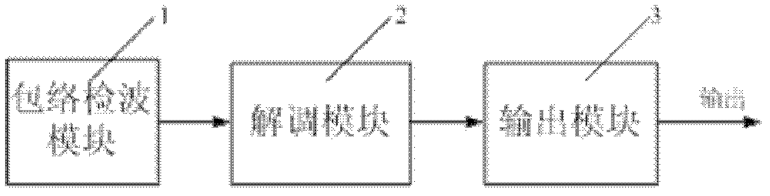
[0029] Please refer to figure 1 , figure 1 It is a schematic structural diagram of the electronic tag demodulation circuit in this embodiment; the electronic tag demodulation circuit includes an envelope detection module 1 and a demodulation module 2 . The envelope wave detection module 1 receives the envelope wave signal in the radio frequency signal and converts the received envelope wave signal into a DC voltage signal and outputs it to the demodulation module 2; The method demodulates the DC voltage signal and outputs the demodulated signal. Further, the electronic label demodulation circuit also includes an output shaping module 3; the output shaping module 3 receives the output signal of the demodulation module, and can perform shaping processing on the demodulated signal; the demodulation module 2 demodulates the output signal Generally, it is not an ideal signal, and the signal power is relatively weak. In order to better output to the subsequent system, the demodula...
Embodiment 2
[0043] Please refer to Figure 6 , Figure 6 It is a circuit structure diagram of the demodulation module of this embodiment; compared with the electronic tag demodulation circuit described in Embodiment 1, in this embodiment, the grid of the third PMOS transistor PM3 of the demodulation module 2 is connected to the first The drains of the three PMOS transistors PM3 are connected to form the input terminal of the second current mirror circuit; the output terminal VD is drawn from the output terminal of the second current mirror (ie, the drain of the fourth PMOS transistor PM4 ).
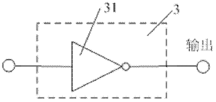
[0044] Further, please refer to Figure 7 , Figure 7 It is a structural schematic diagram of the output shaping module of the present embodiment; the output shaping module 3 includes a Schmitt inverter 31 and a common inverter 32 connected in series with the Schmitt inverter 31, so that the output shaping module The output signal of 3 is consistent with the output signal of demodulation module 2....
Embodiment 3
[0048] Please refer to Figure 8 , Figure 8 It is a schematic structural diagram of an electronic tag in this embodiment; the electronic tag includes an antenna, a rectification module 4, a power supply module 5, a modulation and demodulation module 6, a control module 7 and a storage module 8, and the rectification module 4 receives antenna signals, and receives The battery wave signal is converted into an electrical signal and input into the modulation and demodulation module 6 and the power supply module 5; the power supply module 5 can provide a stable power supply voltage; the modulation and demodulation module 6 includes the Said electronic tag demodulation circuit can demodulate the received signal and output the electronic tag information into the control module; said control module 7 can control the communication system, and the received demodulated electronic tag is sent to the storage Save in the module 8, and read the electronic tag information in the storage mod...
PUM
 Abstract
Description
Claims
Application Information