Defect casual inspection method capable of dynamically adjusting according to technology wafer number load

A dynamic adjustment and defect detection technology, which is applied in semiconductor/solid-state device manufacturing, semiconductor/solid-state device testing/measurement, electrical components, etc., can solve unfavorable production cycle and cost control, lack of wafers to be processed, and increase in the number of wafers and other issues, to achieve the effect of shortening the production cycle, increasing the speed, and avoiding the slowdown of the production speed

Active Publication Date: 2013-10-09
SHANGHAI HUALI MICROELECTRONICS CORP
View PDF6 Cites 13 Cited by
  • Summary
  • Abstract
  • Description
  • Claims
  • Application Information

AI Technical Summary

Problems solved by technology

[0007] In view of the above-mentioned problems, the present invention discloses a defect sampling inspection method that can be dynamically adjusted according to the load of the number of process wafers, so as to overcome the defects in the prior art when the defect inspection equipment stops production for some reason, and t...

Method used


Image

  • Defect casual inspection method capable of dynamically adjusting according to technology wafer number load
  • Defect casual inspection method capable of dynamically adjusting according to technology wafer number load
  • Defect casual inspection method capable of dynamically adjusting according to technology wafer number load

Examples


Embodiment Construction

[0027] The present invention will be further described below in conjunction with the accompanying drawings and specific embodiments, but not as a limitation of the present invention.

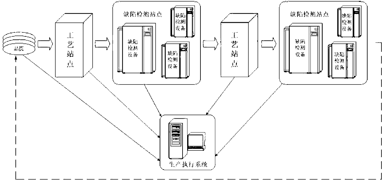
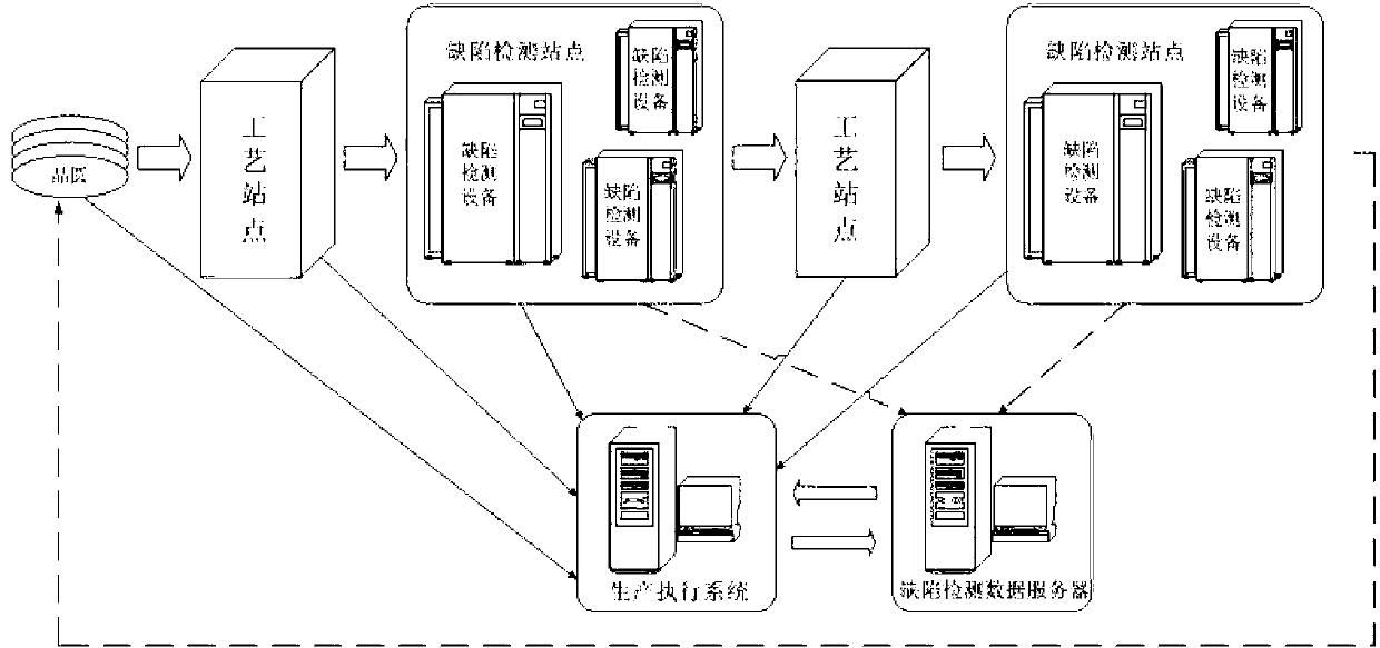
[0028] The first embodiment of the present invention relates to a defect sampling inspection method that can be dynamically adjusted according to the load of the number of process wafers, which is applied to the production execution system and adopts the following steps:

[0029] Step S1, preset in the production execution system as image 3 Defect detection data server shown.

[0030] Step S2, inputting and saving the benchmark sampling frequency of the defect detection site during normal production and the operating rates of different defect detection programs into the defect detection data server.

[0031] Step S3, the defect detection data server calculates the real-time production capacity of the defect detection site according to the real-time status of each defect detection device in the...


PUM


Abstract

The invention discloses a defect casual inspection method capable of dynamically adjusting according to the technology wafer number load. The method comprises the following steps: presetting a defect detection data server; inputting and storing standard casual inspection frequency of a defect detection station and operation speed ratios of different defect detection procedures at normal production time into the defect detection data server; the defect detection data server calculating the real-time capacity of the defect detection station according to the real-time state of each defect detection device in the defect detection station, and automatically upgrading the standard casual inspection frequency of the defect detection station. By the adoption of the method, the problem that dynamic changes of the defect detection capacity cause production speed to become slow and production cost to be increased is effectively avoided. The frequency of defect casual inspection is adjusted according to the dynamic changes of the technology wafer number load, so that integrated circuit production speed is effectively improved, the production period is shortened, and the production cost is eventually reduced.

Description

technical field [0001] The invention relates to the technical field of integrated circuit manufacturing, in particular to a method for sampling wafer defects, in particular to a defect sampling inspection method that can be dynamically adjusted according to the number and load of process wafers. Background technique [0002] The manufacturing process of integrated circuits is very complicated. Simply put, it is to use various methods to form different "layers" on the substrate material (such as silicon substrate), and to dope ions in selected areas to change the semiconductor material. Conductivity, the process of forming a semiconductor device. This process requires many steps to complete. It takes hundreds of processes from wafer to finished integrated circuit. In the actual factory operation, the information automation between wafer and equipment and the execution of process steps are all centered on with the Manufacturing Execution System, such as figure 1 As shown, es...

Claims


Application Information

Patent Timeline
IPC IPC(8): H01L21/66H01L21/67
Inventor 倪棋梁陈宏璘龙吟王恺
Owner SHANGHAI HUALI MICROELECTRONICS CORP
Why Eureka
Try Eureka