Heterojunction, ferroelectric tunnel junction and preparation method and application thereof

A ferroelectric tunnel and heterojunction technology, applied in the field of microelectronic materials, can solve the problems such as the difficulty of direct contact between ferroelectric thin film and semiconductor silicon, and achieve the effects of overcoming the limitation of short shielding length modulation, enhanced tunnel resistance, and good modulation

Inactive Publication Date: 2014-12-10
UNIV OF JINAN
View PDF6 Cites 0 Cited by
  • Summary
  • Abstract
  • Description
  • Claims
  • Application Information

AI Technical Summary

Problems solved by technology

[0006] For metal / ferroelectric / semiconductor FTJ, the most difficult problem is the direct epitaxial integration of ferroelectricity and semiconductor, especially the direct integration of ferroelectricity into mainstream semiconductor silicon, because single crystal silicon semiconductor is easily oxidized in air , it is very difficult to achieve direct contact between ferroelectric thin film and semiconductor silicon

Method used


Image

  • Heterojunction, ferroelectric tunnel junction and preparation method and application thereof

Examples


Embodiment 1

[0051] A method for preparing a ferroelectric / extrinsic silicon semiconductor heterostructure, the preparation steps of which are as follows:

[0052] a) The doped P-type or N-type (001) oriented single crystal silicon semiconductor substrate is cleaned for half an hour by using an ultraviolet ozone cleaner, and then loaded into a molecular beam epitaxy (MBE) chamber.

[0053] b) Use a vacuum pump to pump the vacuum in the growth chamber to 3.0×10 -7 Below Pa.

[0054] c), specifically heating the substrate to 600-700°C and depositing ~ 8 ? thick strontium.

[0055] d), heating the substrate to 750 oC -850oC, SiO 2 The layer desorbs and falls off, and the surface treatment ends when no shedding falls off.

[0056] e), again pumping the vacuum in the growth chamber to 3.0×10 -7 Below Pa.

[0057] f), control the substrate temperature at 300 oC ~350 o Between C.

[0058] g) Precisely control the flux of strontium and titanium flow at 10 16 atoms / m 2 ·s-10 18 atoms / ...

Embodiment 2

[0065] The preparation method of the resistive switching device unit based on metal / ferroelectric / extrinsic silicon semiconductor heterogeneous FTJ, the specific preparation steps are as follows:

[0066]a) Surface treatment and deposition of strontium titanate ferroelectric thin film on doped P-type or N-type (001) oriented single crystal silicon semiconductor substrate according to the method of Example 1.

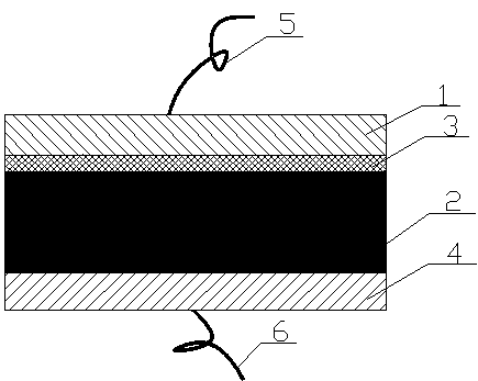
[0067] b) Removal of SrTiO from the MBE growth chamber 3 / (001) Si heterojunction, cover with a mask, and use magnetron sputtering or other coating methods to grow Pt or Au electrodes with a thickness of 100 nm-150 nm;

[0068] c) Print a layer of back electrode on the back of the semiconductor extrinsic silicon substrate: the circular aluminum paste is printed on the whole area, and a 2mm gap is reserved around it, and then the 800 o C-900 o C sintering 50s-60s;

[0069] d) Finally, the lead wires of copper grade and gold are respectively connected from the upper and...


PUM

PropertyMeasurementUnit
thicknessaaaaaaaaaa

Abstract

The invention discloses a heterojunction which comprises a substrate and a ferroelectric film which grows on the substrate in an epitaxial mode, wherein the substrate is an n type doped silicon semiconductor or a p type doped silicon semiconductor, and the ferroelectric film is a SrTiO3 thin film. The invention further discloses a ferroelectric tunnel junction which comprises the heterojunction, wherein an upper electrode covers the surface of the ferroelectric film of the heterojunction, the ferroelectric film of the heterojunction is taken as the barrier layer of the ferroelectric tunnel junction, and the substrate of the heterojunction is taken as a lower electrode of the ferroelectric tunnel junction. The invention further discloses a preparation method and application of the heterojunction and the ferroelectric tunnel junction. According to the heterojunction, direct epitaxial growth of strontium titanate and non-intrinsic silicon is achieved, the stable polarization turning characteristic is expressed, the height of the barrier and the width of the barrier can be adjusted in an electrical modulation mode when the heterojunction is manufactured into the ferroelectric tunnel junction, and therefore the resistance of a tunnel is greatly improved.

Description

technical field [0001] The invention relates to a heterojunction and a preparation method thereof, a ferroelectric tunnel junction and a preparation method thereof, and the application of the ferroelectric tunnel junction in a memristor or a resistive switch device, belonging to the technical field of microelectronic materials. Background technique [0002] A heterojunction is an interface region where two different semiconductors meet. Heterojunctions can be manufactured by interfacial alloys, epitaxial growth, vacuum deposition and other technologies. Heterojunctions often have excellent photoelectric properties, making them suitable for making ultra-high-speed switching devices, solar cells, and semiconductor lasers. The tunnel junction consists of two metal electrodes sandwiched by a nanometer-thick insulating layer (ie, a barrier layer). Quantum mechanics tells us that an electron's wave function can penetrate the barrier with a certain probability. The transmittance ...

Claims


Application Information

Patent Timeline
Patent Type & Authority Patents(China)
IPC IPC(8): H01L45/00
Inventor 杨锋胡广达武卫兵杨长红吴海涛
Owner UNIV OF JINAN
Why Eureka
Try Eureka