Electrowetting display unit on PCB (Printed Circuit Board) and preparation method of electrowetting display unit on PCB
An electrowetting display, PCB board technology, applied in optical components, optics, instruments, etc., can solve problems such as lack of PCB boards, and achieve the effect of saving energy
- Summary
- Abstract
- Description
- Claims
- Application Information
AI Technical Summary
Problems solved by technology
Method used
Image

Examples
Embodiment Construction
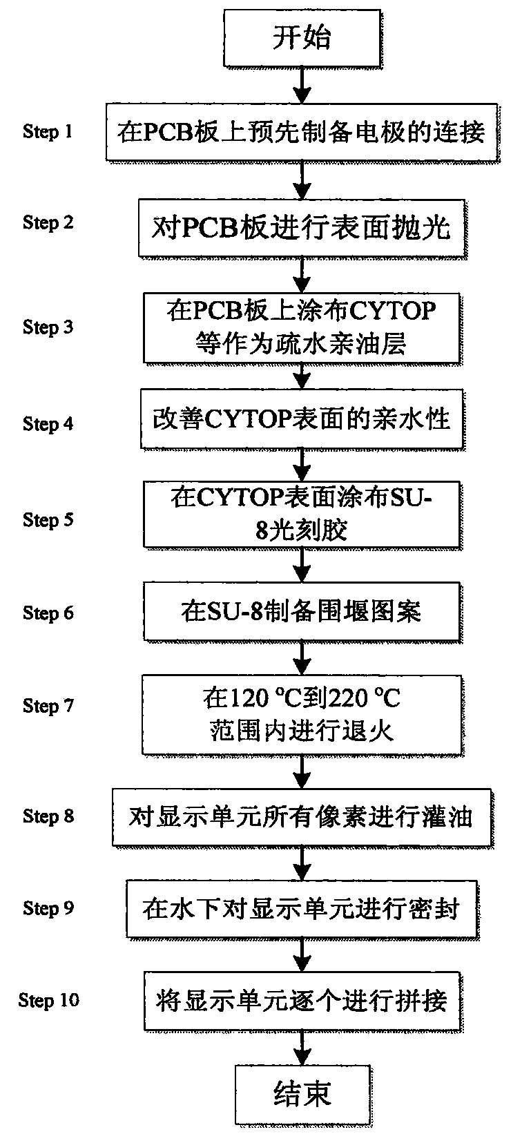
[0025] figure 1 The preparation process of the electrowetting display unit on the PCB provided by the embodiment of the present invention.
[0026] The main production process includes: using the PCB board directly as the base material, polishing the surface, and then preparing it according to the preparation process of the electrowetting display unit.
[0027] There are 10 steps in total.
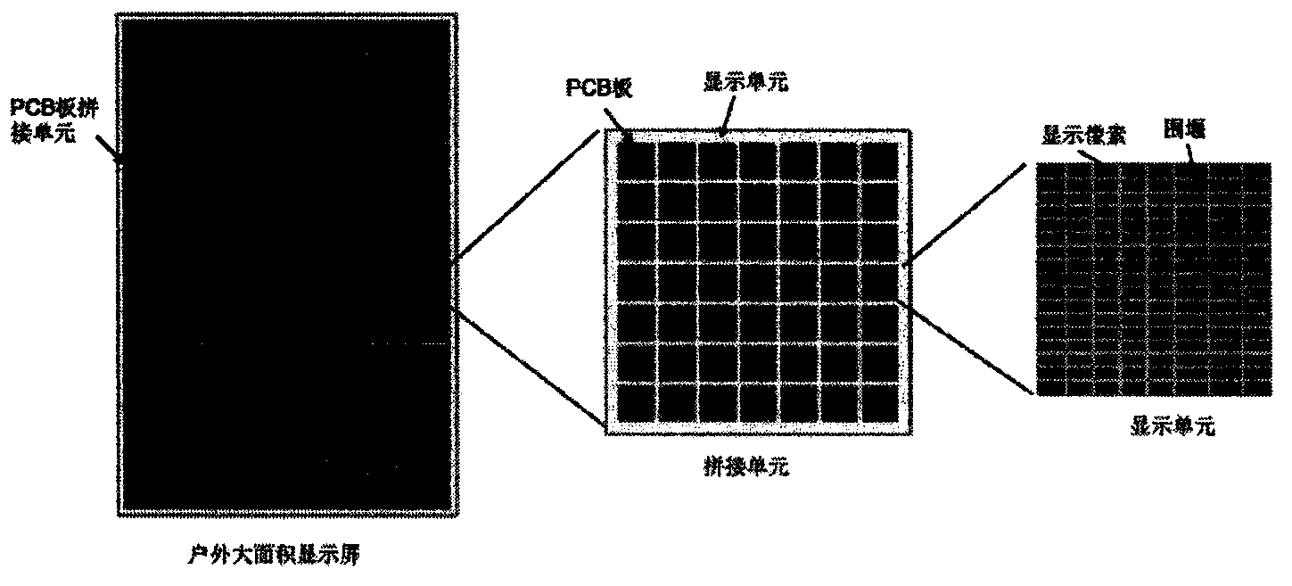
[0028] Step1. Use the standard size PCB board as the splicing unit of the outdoor large-area display, and prepare the electrode connection on the PCB board;
[0029] Step2. Polish the surface of the PCB board, and use magnetron sputtering and other methods to deposit high-reflectivity metal films, such as aluminum films;
[0030] Step3. Coat CYTOP, etc. on the PCB as a hydrophobic and lipophilic layer by spin coating or pulling;
[0031] Step4. Use oxygen plasma to treat the surface to improve the hydrophilicity of CYTOP surface;
[0032] Step5. Apply SU-8 photoresist on the surface of...
PUM
 Abstract
Description
Claims
Application Information
 - R&D
- Intellectual Property
- Life Sciences
- Materials
- Tech Scout
- Unparalleled Data Quality
- Higher Quality Content
- 60% Fewer Hallucinations
Browse by: Latest US Patents, China's latest patents, Technical Efficacy Thesaurus, Application Domain, Technology Topic, Popular Technical Reports.
© 2025 PatSnap. All rights reserved.Legal|Privacy policy|Modern Slavery Act Transparency Statement|Sitemap|About US| Contact US: help@patsnap.com