LED display unit module

A display unit and module technology, applied in electrical components, identification devices, instruments, etc., can solve problems such as limiting LED display technology and LED display technology bottlenecks, and achieve low cost, good thermal stability and flatness, and high stability. sexual effect

Active Publication Date: 2013-10-23
ADVANCED DIGITAL DISPLAY WUXI CO LTD
View PDF4 Cites 10 Cited by
  • Summary
  • Abstract
  • Description
  • Claims
  • Application Information

AI Technical Summary

Problems solved by technology

[0004] However, the traditional LED display technology has a bottleneck in the high-density field
Because it is limited by the traditional structure of the LED light source and the material structure involved in the post-integration processing module, such as the driving capacity and structure of the traditional constant current source package, the loose material of the traditional FR4 PCB board brings the integrated product. The problem of thermal stability, flatness and strength, as well as the injection molded mask and molded case required for installation and splicing into a large screen, etc., all severely limit the application of LED display technology in the high-density field, especially in the display with a pixel pitch of less than 1.0mm. breakthroughs and applications

Method used


Image

  • LED display unit module
  • LED display unit module
  • LED display unit module

Examples


Embodiment Construction

[0030] The technical solutions of the present invention will be described in further detail below with reference to the accompanying drawings and embodiments.

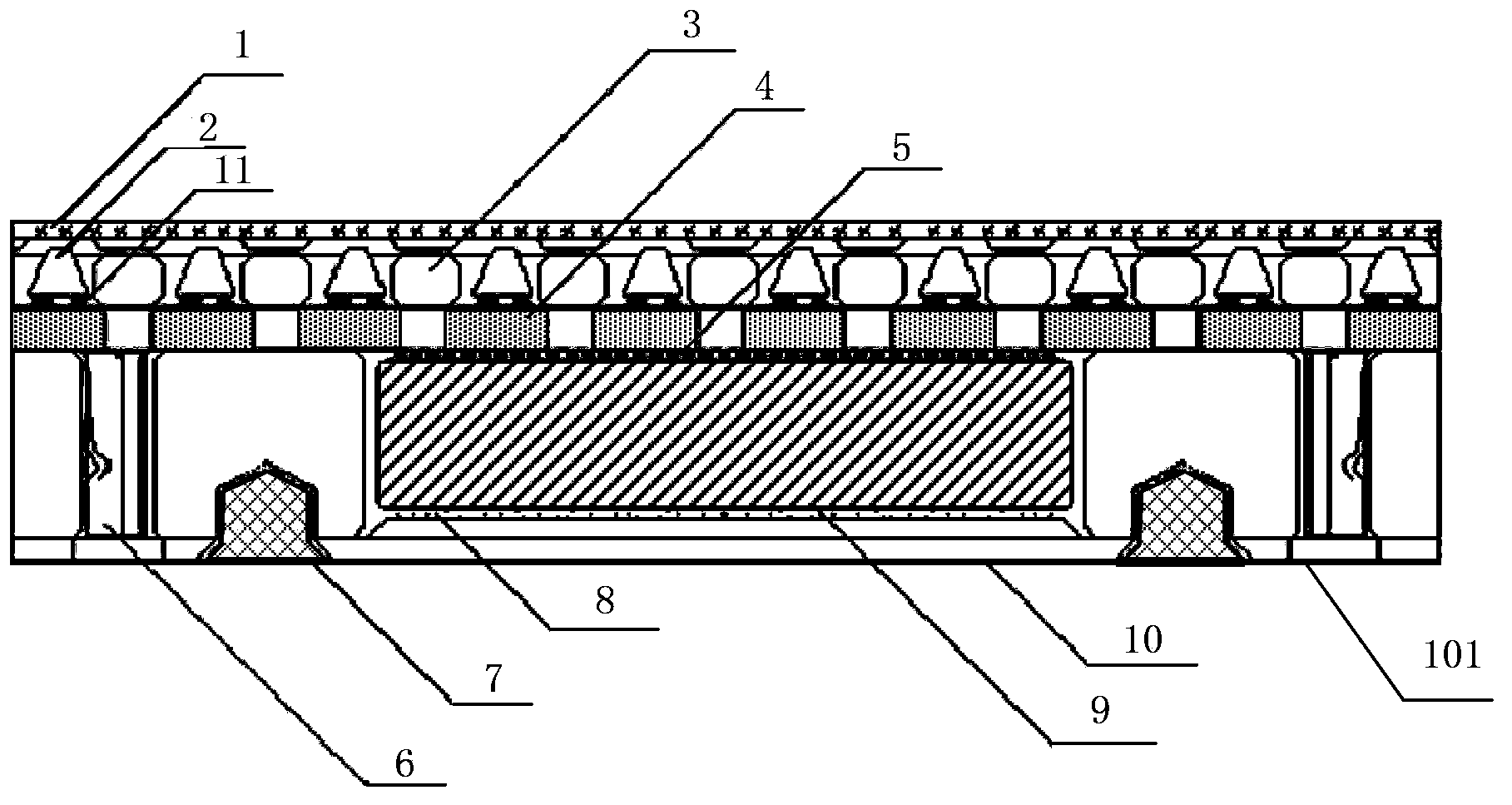
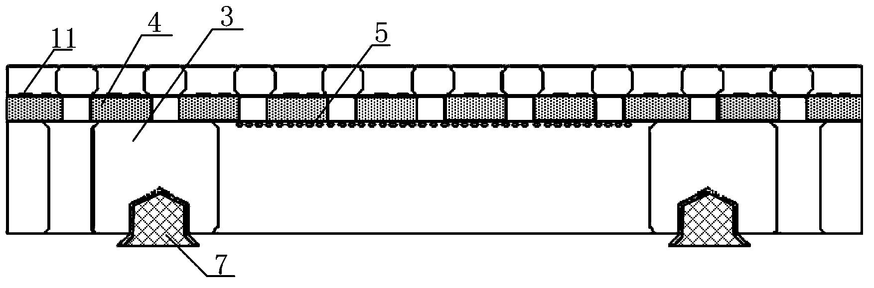
[0031] figure 1 It is a sectional view of the LED display unit module provided by the embodiment of the present invention. Such as figure 1 As shown, the LED display unit module includes: a packaging substrate 4, a chip holder 3, an adhesive layer 11, an interface device 6, a plurality of LED chips 2, an ASIC chip 9, a heat dissipation layer 8 and a heat dissipation cover plate 10;

[0032] The packaging substrate 4 is set in the chip holder 3, and a plurality of LED chips 2 are directly welded (Direct Attach, DA) and eutectic flip-chip is arranged on the top surface of the packaging substrate 4, and connected to the packaging substrate 4 through the adhesive layer 11; dedicated integration The circuit chip 9 is flip-chip arranged on the bottom surface of the packaging substrate 4, connected to the packaging substrat...


PUM


Abstract

The invention relates to an LED display unit module which comprises a packaging substrate, a wafer support, a bonding layer, an interface device, a plurality of LED chips, an application-specific integrated circuit chip, a heat dissipating layer and a heat dissipating cover plate, wherein the packaging substrate is arranged inside the wafer support, the top surface and the bottom surface of the packaging substrate are used for loading a plurality of reversed LED chips and reversed application-specific integrated circuit chip, the LED chips are electrically connected with the packaging substrate through the bonding layer; the application-specific integrated circuit chip is electrically connected with the packaging substrate through the ball grid array BGA technology or the bonding layer; the LED chips are electrically connected with the application-specific integrated circuit chip through the packaging substrate; the heat dissipating cover plate is fixed on the outer side of the application-specific integrated circuit chip through the heat dissipating layer and is especially used for heat dissipating of the application-specific integrated circuit chip; the interface device is arranged in the chip support between the bottom surface of the packaging substrate and the heat dissipating cover plate, is exposed through an opening formed in the heat dissipating cover plate, and is used for electrical connection between the packaging substrate and the external circuit.

Description

technical field [0001] The invention relates to the field of semiconductors, in particular to an LED display unit module. Background technique [0002] In the past ten years, there have been two directional changes in the display field. Around 2000, the cathode ray tube (CRT) industry faced a crisis of substitution. After that, the mainstream direction tends to plasma display (PDP) and thin film transistor liquid crystal display (TFT-LCD). After more than 10 years of development, TFT-LCD has become the mainstream in the display field. Then, with the advancement of TFT-LCD and electroluminescence (EL) technology, active organic light-emitting display (AMOLED) also began to be industrialized. In addition, new display technologies such as Flexible Display and Laser Display continue to emerge. At present, a new round of debate about the development direction of the display industry has begun again. No matter from the perspective of TFT-LCD or AMOLED development, we can clea...

Claims


Application Information

Patent Timeline
Patent Type & Authority Applications(China)
IPC IPC(8): G09F9/33H01L21/58H01L21/60
CPCH01L24/18H01L2224/04105H01L2224/12105H01L2224/16227H01L2224/20H01L2224/32245H01L2224/73267H01L2224/92244H01L2924/01322H01L2924/00H01L2224/18H01L2924/00012
Inventor 严敏程君周鸣波
Owner ADVANCED DIGITAL DISPLAY WUXI CO LTD
Why Eureka
Try Eureka