LED (Light-Emitting Diode) chip with high luminous efficiency and manufacturing method thereof

A technology of light-emitting diodes and manufacturing methods, applied to electrical components, circuits, semiconductor devices, etc., to achieve the effects of reducing total reflection, improving light extraction efficiency, and improving luminous efficiency

Inactive Publication Date: 2013-10-23
EPITOP PHOTOELECTRIC TECH
View PDF6 Cites 6 Cited by
  • Summary
  • Abstract
  • Description
  • Claims
  • Application Information

AI Technical Summary

Problems solved by technology

However, there is still no technology that can better solve this problem

Method used


Image

  • LED (Light-Emitting Diode) chip with high luminous efficiency and manufacturing method thereof

Examples


Embodiment 1

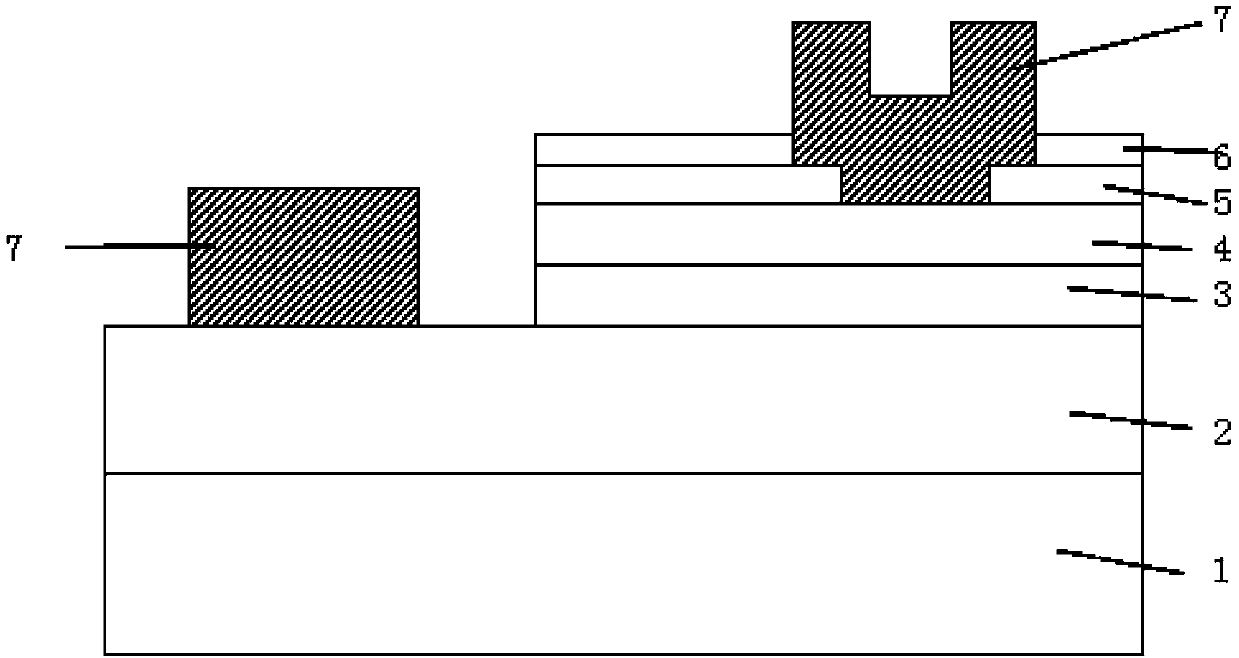
[0019] 1. On the sapphire substrate 1, grow the N-type GaN layer 2, the active layer 3 and the P-type GaN layer 4 in sequence, and remove part of the P-type GaN layer 4 and the active layer 3 by etching to expose a part of the N-type GaN layer 2.

[0020] 2. Evaporating a current spreading layer 5 on the P-type GaN layer 4 by means of electron beam evaporation. In this embodiment, the current spreading layer 5 is an ITO thin film layer. SnO in ITO evaporation source 2 with In 2 o 3 The mass percentage is 10:90, and the vacuum degree is 1.8×10 -5 Torr, the chamber temperature was maintained at 250 °C. first step, O 2 The flow rate is set to 15 sccm, the evaporation rate is 0.1 nm / s, the thickness is set to 57.4 nm, and the ITO film layer with a refractive index of about 2 is set. In the second step, O 2 The flow rate is set to 3 sccm, the evaporation rate is set to 0.15 nm / s, and the thickness is set to 66.5 nm to form an ITO thin film layer with a refractive index of ab...

Embodiment 2

[0024] 1. On the sapphire substrate 1, grow the N-type GaN layer 2, the active layer 3 and the P-type GaN layer 4 in sequence, and remove part of the P-type GaN layer 4 and the active layer 3 by etching to expose a part of the N-type GaN layer 2.

[0025] 2. Evaporating a current spreading layer 5 on the P-type GaN layer 4 by means of electron beam evaporation. In this embodiment, the current spreading layer 5 is an ITO thin film layer. SnO in ITO evaporation source 2 with In 2 o 3 The mass percentage is 5:95, and the vacuum degree is 1.8×10 -5 Torr, the chamber temperature was maintained at 250 °C. first step, O 2 The flow rate is set at 15 sccm, the evaporation rate is 0.2nm / s, the thickness is set at 56nm, and the ITO film layer with a refractive index of about 2.05. In the second step, O 2 The flow rate is set to 3 sccm, the evaporation rate is set to 0.25nm / s, and the thickness is set to 65.7nm to form an ITO film layer with a refractive index of about 1.72.

[00...

Embodiment 3

[0029] 1. On the sapphire substrate 1, grow the N-type GaN layer 2, the active layer 3 and the P-type GaN layer 4 in sequence, and remove part of the P-type GaN layer 4 and the active layer 3 by etching to expose a part of the N-type GaN layer 2.

[0030] 2. Evaporating a current spreading layer 5 on the P-type GaN layer 4 by means of electron beam evaporation. In this embodiment, the current spreading layer 5 is an ITO thin film layer. SnO in ITO evaporation source 2 with In 2 o 3 The mass percentage is 10:90, and the vacuum degree is 1.8×10 -5 Torr, the chamber temperature was maintained at 250 °C. first step, O 2 The flow rate is set to 12sccm, the evaporation rate is 0.1nm / s, the thickness is set to 58.9nm, and the ITO film layer with a refractive index of about 1.95. The second step 2The flow rate is set to 4sccm, the evaporation rate is set to 0.25nm / s, and the thickness is set to 65.3nm to form an ITO film layer with a refractive index of about 1.73.

[0031] 3....


PUM


Abstract

The invention provides an LED (Light-Emitting Diode) chip with high luminous efficiency. The LED chip comprises an N-type semiconductor layer, an active layer, a P-type semiconductor layer, a current expanding layer and an insulating covering layer sequentially arranged on a substrate, wherein the refractive index value of the current expanding layer is between the refractive index values of the P-type semiconductor layer and the insulating covering layer and is distributed in gradient along the direction vertical to the current expanding layer to reduce the difference between the refractivity at the interface of the current expanding layer and the insulating covering layer and the refractivity at the interface of the current expanding layer and the P type semiconductor layer so as to reduce the total reflection at the interface. The LED chip provided by the invention has the advantages that the generation of the total reflection is reduced by forming the current expanding layer with the gradient change of the refractivity to obtain more emergent light so as to improve the luminous efficiency of the chip.

Description

technical field [0001] The invention belongs to the field of semiconductor devices, and in particular relates to a light-emitting diode chip and a manufacturing method thereof, in particular to a light-emitting diode chip with an ITO thin film layer with a gradient change in refractive index and a manufacturing method thereof. technical background [0002] Semiconductor lighting is an emerging technology, which has outstanding advantages such as environmental protection, energy saving and safety, and is the star of hope for the new generation of lighting. Light-emitting diode (LED) is a light-emitting device that converts electrical energy into light energy, and is widely used in many fields such as indication, display, decoration, and lighting. And, due to its outstanding energy saving and environmental protection characteristics and increasing luminous efficiency, it is more and more used in the field of general lighting and LCD backlight. However, in order to obtain a br...

Claims


Application Information

Patent Timeline
Patent Type & Authority Applications(China)
IPC IPC(8): H01L33/14H01L33/00
Inventor 陈静康建郑远志陈向东李晓莹
Owner EPITOP PHOTOELECTRIC TECH
Why Eureka
Try Eureka