Interface charge compensation Schottky semiconductor device and manufacturing method for same

A technology of interface charges and conductive semiconductors, applied in semiconductor/solid-state device manufacturing, semiconductor devices, circuits, etc., can solve problems such as low forward turn-on voltage, fast turn-on and turn-off speed, and influence on device reverse breakdown characteristics

Inactive Publication Date: 2013-11-06
朱江
View PDF6 Cites 3 Cited by
  • Summary
  • Abstract
  • Description
  • Claims
  • Application Information

AI Technical Summary

Problems solved by technology

[0002] Power semiconductor devices are widely used in power management and power applications, especially semiconductor devices involving Schottky junctions have become an important trend in device development. Schottky devices have the advantages of low forward turn-on voltage and fast turn-on and turn-off speed. At the same time, Schottky devices also have the disadvantages of large reverse leakage current and cannot be used in high-voltage environments.
[0003] Schottky diodes can be manufactured through a variety of different layout techniques, the most commonly used is planar layout, the traditional planar Schottky diode has a sudden electric field distribution curve in the drift region, which affects the reverse breakdown characteristics of the device, while the traditional The planar Schottky diode has a high on-resistance

Method used


Image

  • Interface charge compensation Schottky semiconductor device and manufacturing method for same
  • Interface charge compensation Schottky semiconductor device and manufacturing method for same
  • Interface charge compensation Schottky semiconductor device and manufacturing method for same

Examples


Embodiment 1

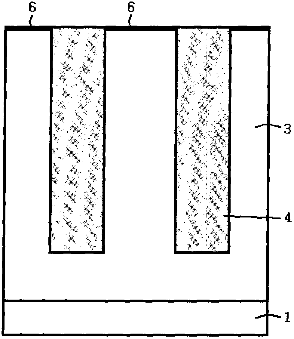
[0019] figure 1 It is a sectional view of an interface charge compensation Schottky semiconductor device of the present invention, combined below figure 1 The semiconductor device of the present invention will be described in detail.

[0020] An interface charge compensation Schottky semiconductor device, comprising: a substrate layer 1, which is an N conductivity type semiconductor silicon material, and the doping concentration of phosphorus atoms is 1E19 / CM 3 ; The first conductive semiconductor material 3, located on the substrate layer 1, is a semiconductor silicon material of N conductivity type, and the doping concentration of phosphorus atoms is 1E16 / CM 3 Oxygen-doped polysilicon 4 located in the first conductive semiconductor material 3 ; Schottky barrier junction 6 located on the surface of the first conductive semiconductor material 3 .

[0021] Its manufacturing process includes the following steps:

[0022] In the first step, a first conductive semiconductor mat...

Embodiment 2

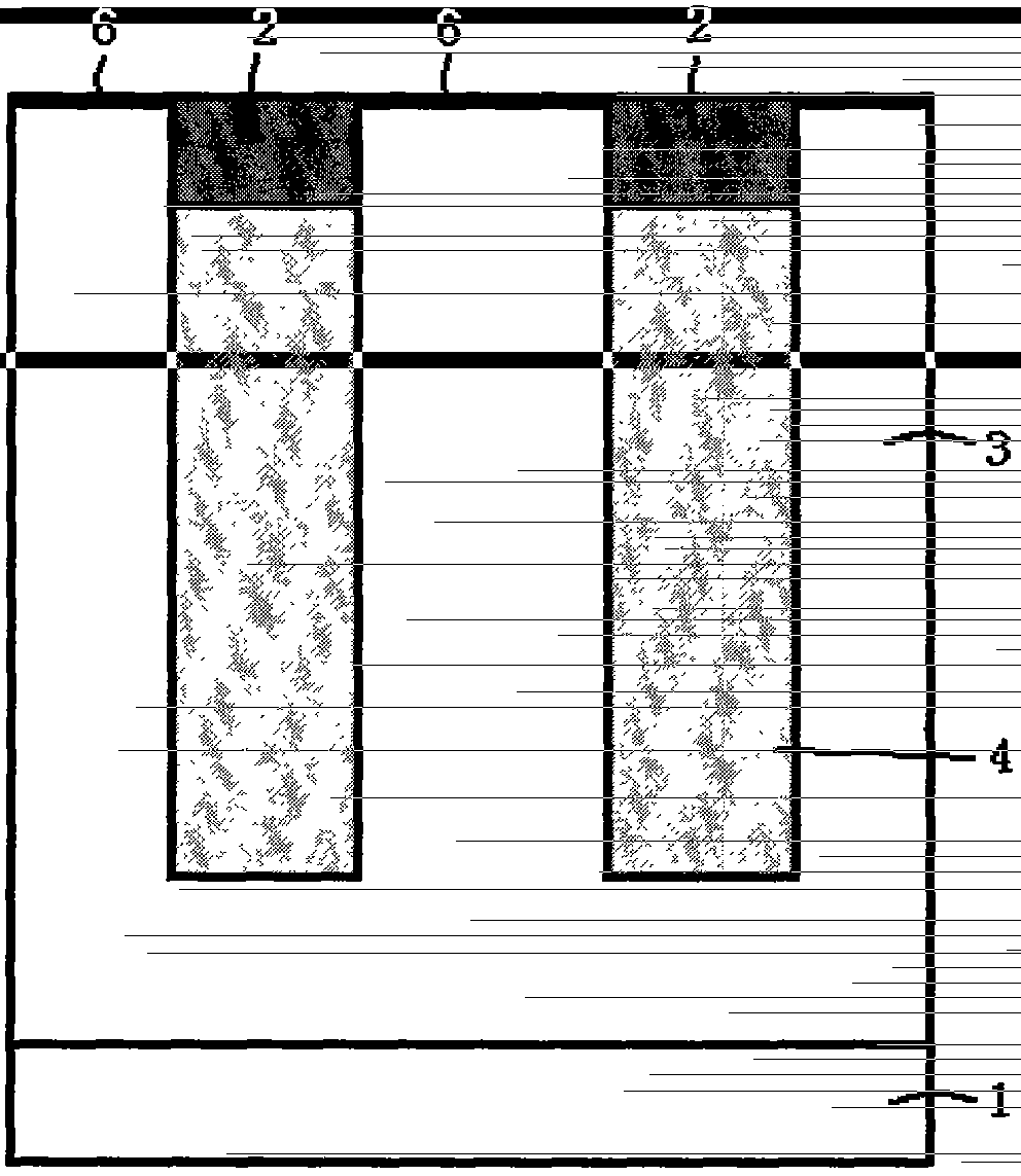
[0027] figure 2 It is a sectional view of the second interface charge compensation Schottky semiconductor device of the present invention, combined below figure 2 The semiconductor device of the present invention will be described in detail.

[0028] An interface charge compensation Schottky semiconductor device, comprising: a substrate layer 1, which is an N conductivity type semiconductor silicon material, and the doping concentration of phosphorus atoms is 1E19 / CM 3 ; The first conductive semiconductor material 3, located on the substrate layer 1, is a semiconductor silicon material of N conductivity type, and the doping concentration of phosphorus atoms is 1E16 / CM 3 Oxygen-doped polysilicon 4, located in the first conductive semiconductor material 3; Schottky barrier junction 6, located on the surface of the first conductive semiconductor material 3; silicon dioxide 2, located on the upper surface of the first conductive semiconductor material 3.

[0029] Its manufactu...

Embodiment 3

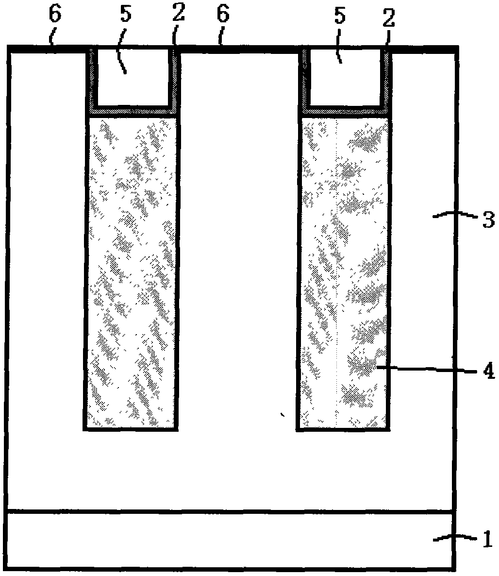
[0036] image 3 It is a sectional view of the third interface charge compensation Schottky semiconductor device of the present invention, combined below image 3 The semiconductor device of the present invention will be described in detail.

[0037] An interface charge compensation Schottky semiconductor device, comprising: a substrate layer 1, which is an N conductivity type semiconductor silicon material, and the doping concentration of phosphorus atoms is 1E19 / CM 3 ; The first conductive semiconductor material 3, located on the substrate layer 1, is a semiconductor silicon material of N conductivity type, and the doping concentration of phosphorus atoms is 1E16 / CM 3 Oxygen-doped polysilicon 4, located in the first conductive semiconductor material 3; Schottky barrier junction 6, located on the surface of the first conductive semiconductor material 3; silicon dioxide 2, located on the upper surface of the first conductive semiconductor material 3; polycrystalline The secon...


PUM


Abstract

The invention discloses an interface charge compensation Schottky semiconductor device. When the semiconductor device is connected with a certain reverse biased voltage, charge compensation is generated by interface charge compensation regions and drifting semiconductor materials, depletion layers between the interface charge compensation regions are made to be overlapped, and therefore the reverse breakdown voltage of the device is improved, or the forward breakover resistance of the device is lowered, and the forward breakover feature of the device is improved. The invention further provides a manufacturing method for the interface charge compensation Schottky semiconductor device.

Description

technical field [0001] The invention relates to an interface charge compensation Schottky semiconductor device, and also relates to a preparation method of the interface charge compensation Schottky semiconductor device. The semiconductor device of the present invention is a basic structure for manufacturing power rectifying devices. Background technique [0002] Power semiconductor devices are widely used in power management and power applications, especially semiconductor devices involving Schottky junctions have become an important trend in device development. Schottky devices have the advantages of low forward turn-on voltage and fast turn-on and turn-off speed. At the same time, Schottky devices also have disadvantages such as large reverse leakage current and cannot be used in high-voltage environments. [0003] Schottky diodes can be manufactured through a variety of different layout techniques, the most commonly used is planar layout, the traditional planar Schottky...

Claims


Application Information

Patent Timeline
Patent Type & Authority Applications(China)
IPC IPC(8): H01L29/872H01L21/329
Inventor 朱江
Owner 朱江
Why Eureka
Try Eureka