Light-emitting diode (LED) packaged with AlSiC composite substrate
A composite substrate, LED light source technology, applied in electrical components, circuits, semiconductor devices, etc., can solve the problems of low reactivity of metals and ceramics, poor wettability of metals and ceramics, and high requirements for forming dimensional accuracy, and achieves a suitable size for large Large-scale production, high specific stiffness, and the effect of improving reflectivity
- Summary
- Abstract
- Description
- Claims
- Application Information
AI Technical Summary
Problems solved by technology
Method used
Image
Examples
Embodiment
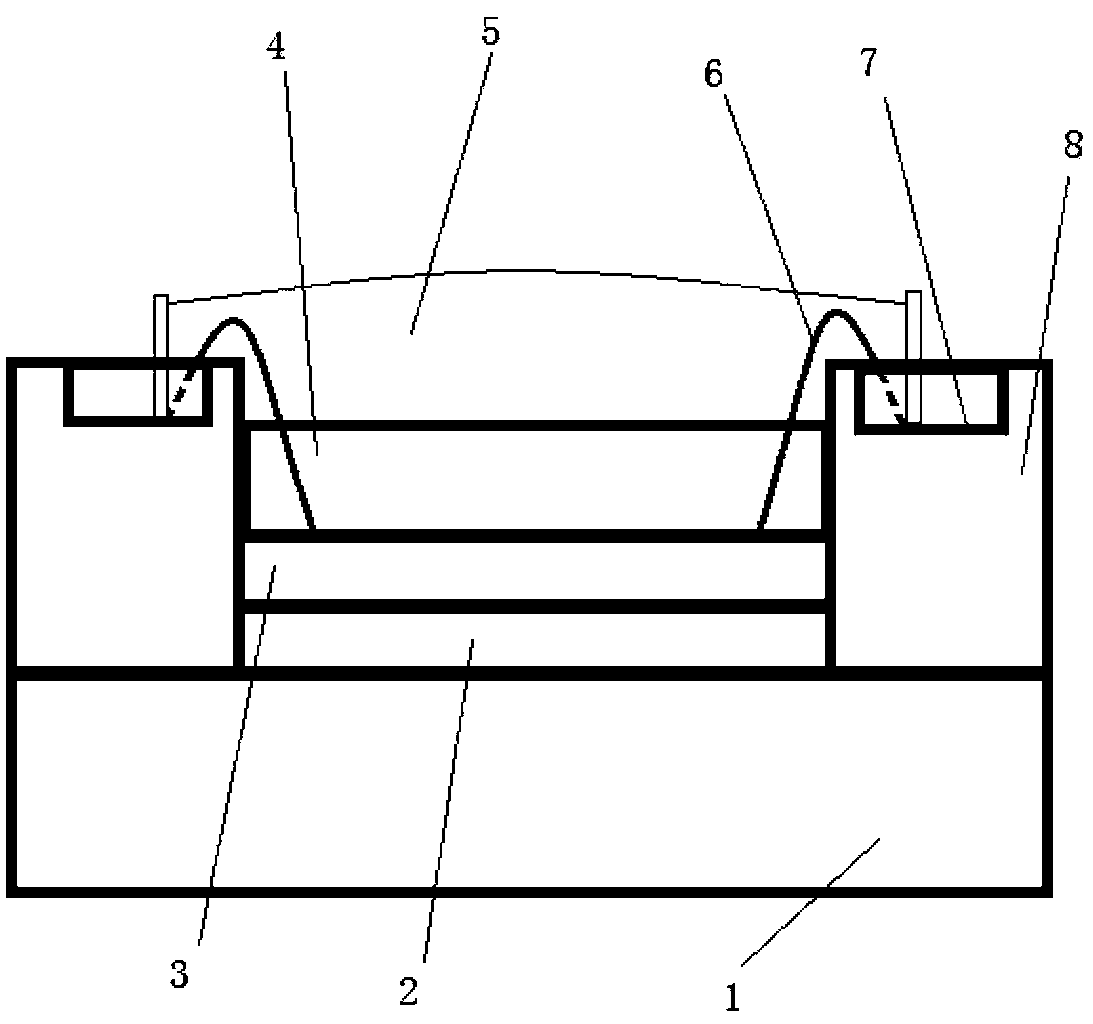
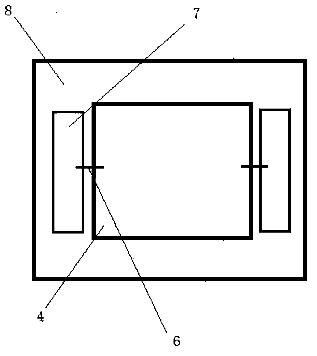
[0020] Such as Figure 1~2 As shown, an LED packaged with an AlSiC composite substrate of this embodiment includes an AlSiC composite heat dissipation substrate 1, an LED light source module 4, a gold wire 6 and an alumina ceramic frame 8 on which a copper film 2 and a silver film 3 are sequentially plated on the surface. The LED light source module 4 is packaged on the AlSiC composite heat dissipation substrate 1 using COB packaging technology; the alumina ceramic frame 8 is arranged on the outside of the LED light source module 4 and is bonded to the LED light source module 4; the alumina ceramic frame 8 Two copper film electrodes 7 are plated on the surface. The two copper film electrodes 7 are respectively connected to the positive and negative electrodes of the LED light source module 4 through a gold wire 6. The transparent silica gel 5 wraps the gold wire 6, and the copper film electrode 7 is connected to the gold wire 6. section.
[0021] The copper film includes a first...
Embodiment 2
[0030] This embodiment has the same features as the first embodiment except for the following features.
[0031] The thickness of the first layer of copper film of the LED packaged with the AlSiC composite substrate of this embodiment is 1 μm, and the thickness of the second layer of copper film is 20 μm.
PUM
| Property | Measurement | Unit |
|---|---|---|
| thickness | aaaaa | aaaaa |
| thickness | aaaaa | aaaaa |
| thickness | aaaaa | aaaaa |
Abstract
Description
Claims
Application Information

