Nitride semiconductor device

A nitride semiconductor and semiconductor technology, which is applied in the direction of semiconductor devices, semiconductor/solid-state device manufacturing, electrical components, etc., can solve the problem of not increasing the longitudinal withstand voltage of semiconductor devices, the switching characteristics of semiconductor devices, and the influence of high-frequency characteristics on electrical characteristics, etc. question

Active Publication Date: 2013-11-13
PANASONIC INTELLECTUAL PROPERTY MANAGEMENT CO LTD
View PDF4 Cites 2 Cited by
  • Summary
  • Abstract
  • Description
  • Claims
  • Application Information

AI Technical Summary

Problems solved by technology

It has also been found that not only Si substrates but also other semiconductor substrates such as silicon carbide (SiC) substrates and gallium arsenide (GaAs) substrates have the same problem
Furthermore, it was found that the reason why the vertical withstand voltage of the semiconductor device cannot be increased is that it also affects the electrical characteristics such as switching characteristics and high-frequency characteristics of the semiconductor device.

Method used


Image

  • Nitride semiconductor device
  • Nitride semiconductor device
  • Nitride semiconductor device

Examples


Embodiment Construction

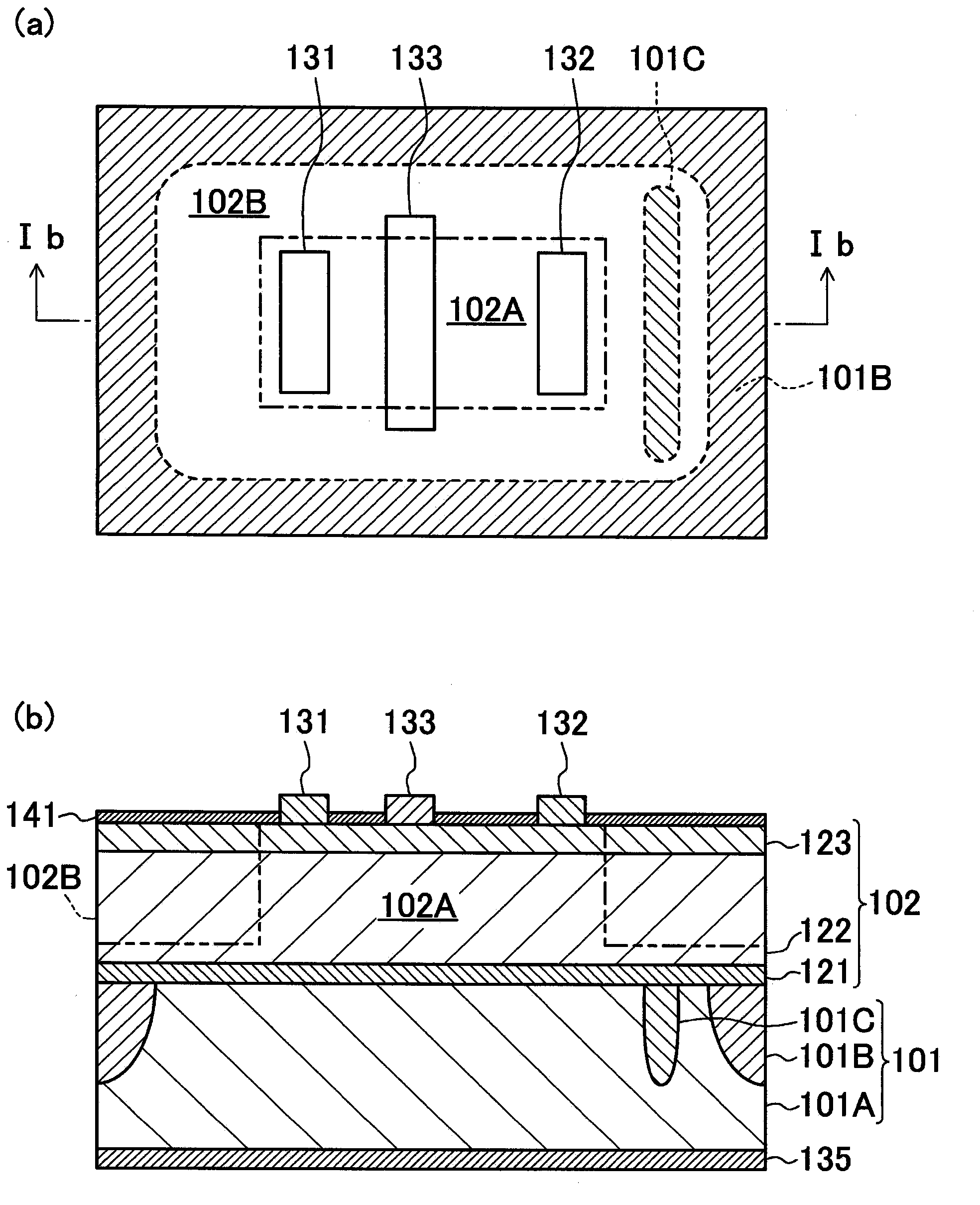
[0049] In this specification, AlGaN means ternary mixed crystal Al x Ga 1-x N (here, 0≤x≤1). The multi-component mixed crystal is abbreviated as the arrangement of symbols of the respective constituent elements, for example, AlInN, GaInN and the like. For example, nitride semiconductor Al x Ga 1-x-y In y N (here, 0≤x≤1, 0≤y≤1, x+y≤1) is abbreviated as AlGaInN. In addition, undoped means that no impurities are intentionally introduced.

[0050] First, the relationship between the withstand voltage of a semiconductor substrate and the vertical withstand voltage of a semiconductor device discovered by the inventors of the present application will be described.

[0051] First, as a semiconductor device for evaluation, a nitride semiconductor layer with a predetermined film thickness is formed on various p-type Si substrates and n-type Si substrates having different carrier (impurity) concentrations. The withstand voltage was measured. The vertical breakdown voltage of the ...


PUM


Abstract

This nitride semiconductor device is provided with a semiconductor substrate (101) and a nitride semiconductor layer (102) formed on the semiconductor substrate. The semiconductor substrate (101) comprises a normal region (101A), carrier supply region(s) (101C), and an interface current blocking region (101B). The interface current blocking region surrounds the normal region and carrier supply region(s), and the interface current blocking region and carrier supply region(s) each contain impurities. The carrier supply region(s) forms a source for supplying carriers to a carrier layer formed at the interface between the nitride semiconductor layer and the semiconductor substrate and has a conductivity type that forms an elimination destination for the carriers. The interface current blocking region is of a conductivity type that forms a potential barrier for the carriers.

Description

technical field [0001] The present invention relates to a nitride semiconductor device, and more particularly, to a semiconductor device using a nitride semiconductor that can be applied as a power transistor used in a power supply circuit or the like. Background technique [0002] Nitride semiconductors typified by gallium nitride (GaN) are attracting attention as materials for high-frequency semiconductor devices or high-output semiconductor devices. Research on using a silicon (Si) substrate or the like as a substrate for forming a semiconductor device using a nitride semiconductor is ongoing. The Si substrate can easily achieve a larger diameter, and if the Si substrate is used as the substrate on which the nitride semiconductor is grown, the cost of the semiconductor device using the nitride semiconductor can be greatly reduced. [0003] When forming a semiconductor device using a nitride semiconductor on a Si substrate, the potential of the Si substrate affects the op...

Claims


Application Information

Patent Timeline
Patent Type & Authority Applications(China)
IPC IPC(8): H01L21/338H01L29/47H01L29/778H01L29/812H01L29/872
CPCH01L29/7781H01L29/2003H01L29/0607H01L29/0692H01L29/41725H01L29/7786H01L29/861
Inventor 梅田英和上田哲三上田大助
Owner PANASONIC INTELLECTUAL PROPERTY MANAGEMENT CO LTD
Why Eureka
Try Eureka