Microlens, microlens array structure and manufacturing process thereof

An array structure and microlens technology, applied in microstructure technology, microstructure devices, manufacturing microstructure devices, etc., can solve the problems of low resolution, crosstalk, incomplete image distinction, etc., to improve resolution, reduce crosstalk, Distinguish obvious effects

Active Publication Date: 2013-11-20
SOUTHEAST UNIV
View PDF4 Cites 17 Cited by
  • Summary
  • Abstract
  • Description
  • Claims
  • Application Information

AI Technical Summary

Problems solved by technology

[0002] Integrated imaging technology is becoming more and more mature, but there are still some key technical problems in the current integrated imaging display: in the acquisition process, the preparation of large size, uniform focal length, and large crosstalk is a key technology that restricts integrated imaging stereoscopic display
At present, three-dimensional imaging technology often adopts multi-viewpoint technology to obtain better stereoscopic effects, and uses traditional microlens arrays with pixels as viewpoints to form a field of view with three adjacent sub-pixels, but this array structure is prone to Incomplete image differentiation, resulting in crosstalk and low resolution

Method used


Image

  • Microlens, microlens array structure and manufacturing process thereof
  • Microlens, microlens array structure and manufacturing process thereof
  • Microlens, microlens array structure and manufacturing process thereof

Examples


Embodiment approach

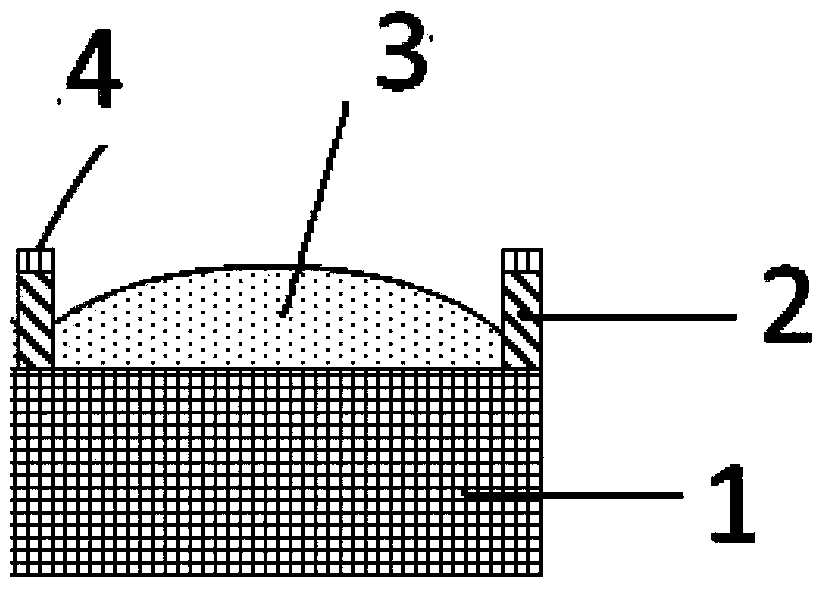
[0039] Microlens array is an optical device widely used in three-dimensional stereoscopic display. The microlens array is used in the acquisition stage and reproduction stage of integrated imaging, and its size, shape, focal length and other parameters have an important impact on the image display quality. Therefore, the preparation of a microlens array that meets the requirements is very critical for the research of integrated imaging. The manufacturing process of the present invention mainly has five steps. In the manufacturing process, each step requires high precision, so that the manufactured microlens array can have good uniformity and consistent optical characteristics. The method of implementation is as follows:

[0040] (1) Lamination

[0041] Microlens arrays are generally fabricated on glass substrates, first by cleaning the glass substrates and cutting them into required dimensions. Then, the photoresist is pressed on the glass substrate with a lamination machin...


PUM

PropertyMeasurementUnit
thicknessaaaaaaaaaa

Abstract

The invention discloses a sub-pixel microlens liquid lens array structure, wherein microlens subgraphs are arranged once again by taking red, green and blue sub-pixels as viewpoints, and a lens is prepared via arranging the sub-pixels once again; the individual lens in the microlens array structure is rectangular, and rows can be staggered. The physical structure of each lens comprises a bottom substrate, a cavity structure is built on the substrate, and a solidified liquid is in the cavity structure. The upper surface of the side wall of each cavity structure comprises a drainage zone; the drainage zone has physical property repelling the liquid to ensure the liquid in the cavities not to slide onto the side walls. The invention further provides a manufacturing process of the sub-pixel microlens liquid lens array structure, and the structure is easy to implement, is low in manufacturing cost, and has very strong practicability.

Description

technical field [0001] The invention relates to a subpixel microlens liquid lens array structure, in particular to a subpixel microlens liquid lens array structure after rearranging microlens subimages with red, green and blue subpixels as viewpoints. Background technique [0002] Integrated imaging technology is becoming more and more mature, but there are still some key technical problems in the current integrated imaging display: in the acquisition process, the preparation of large size, uniform focal length, and large crosstalk is a key technology that restricts integrated imaging stereoscopic display. In the reconstruction process, the true 3D image reconstructed by the microlens array has problems such as small depth of field, narrow viewing angle, and low resolution. [0003] Existing imaging technologies generally adopt the RGB color mode. RGB is the color representing the three channels of red, green, and blue (hereinafter referred to as RGB). This standard includes...

Claims


Application Information

Patent Timeline
Patent Type & Authority Applications(China)
IPC IPC(8): G02B3/12G02B3/00B81C1/00
Inventor 夏军杨鑫李清蓉王保平
Owner SOUTHEAST UNIV
Why Eureka
Try Eureka