Formation method of flash memory storage unit

A flash memory storage and sacrificial layer technology, applied in electrical components, semiconductor/solid-state device manufacturing, circuits, etc., can solve the problem of poor erase performance of flash memory cells, poor stability of chips or integrated circuits, and difficult to control top 19 topography. and other problems, to achieve the same top shape, uniform structure, and stable performance.

Active Publication Date: 2013-11-20
SHANGHAI HUAHONG GRACE SEMICON MFG CORP
View PDF3 Cites 13 Cited by
  • Summary
  • Abstract
  • Description
  • Claims
  • Application Information

AI Technical Summary

Problems solved by technology

[0004] However, the angular size of the tip 19 formed in the prior art is inaccurate, and the shape of the tip 19 is difficult to control, resulting in poor erasing performance of the formed flash memory storage unit, and poor stability of the chip or integrated circuit

Method used


Image

  • Formation method of flash memory storage unit
  • Formation method of flash memory storage unit
  • Formation method of flash memory storage unit

Examples


Embodiment Construction

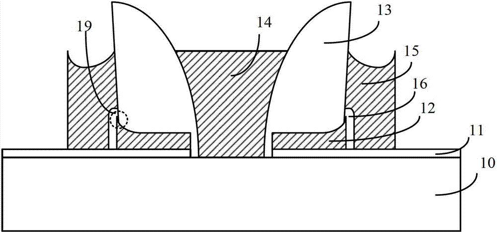
[0028] As mentioned in the background, the top angle dimension of the floating gate layer formed in the prior art is inaccurate, the shape of the top is difficult to control, the erase performance of the formed flash memory storage unit is poor, and the stability of the chip or integrated circuit is not good.

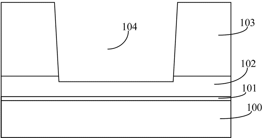
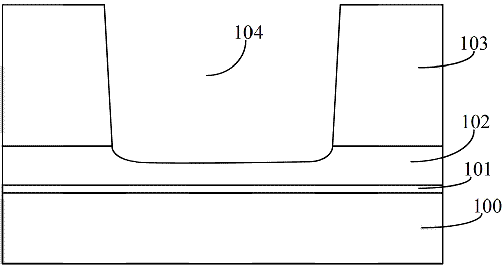
[0029] Figure 2 to Figure 5 is formed as figure 1 A schematic diagram of the cross-sectional structure of the process of the floating gate layer, the sidewall and the source line layer of the storage unit of the flash memory.

[0030] Please refer to figure 2 , provide a semiconductor substrate 100, the surface of the semiconductor substrate 100 has a tunnel oxide layer 101, a floating gate film 102 on the surface of the tunnel oxide layer 101, and a dielectric layer 103 on the surface of the floating gate film 102; using anisotropic The dielectric layer 103 and part of the floating gate film 102 are etched by a dry etching process to form a first opening 104 so tha...


PUM


Abstract

The invention relates to a formation method of a flash memory storage unit. The formation method comprises the following steps: providing a plurality of batches of semiconductor structures, wherein each semiconductor structure comprises a substrate, a tunneling oxide layer positioned on the surface of the substrate, a floating gate layer positioned on the surface of the tunneling oxide layer, a sacrificial layer positioned on the surface of the floating gate layer, and a mask layer positioned on the surface of the sacrificial layer, and the mask layer is exposed out of partial surface of the sacrificial layer; etching sacrificial layers and partial floating gate layers in each batch in sequence with an anisotropic dry method by taking a mask layer as a mask, and forming first openings in the sacrificial layers and the floating gate layers in each batch, wherein a determination method of the etching time of a batch to be etched comprises obtaining the etching time of the batch to be etched by the thickness of the sacrificial layer of a batch prior to the batch to be etched, the etching thickness of the floating gate layer of the batch prior to the batch to be etched, and the thickness of the sacrificial layer of the batch to be etched. According to the method, the top sizes of bulges on the top surface of the floating gate layer of each batch are accurate and uniform, so that the erasing performance of the flash memory storage unit is improved.

Description

technical field [0001] The invention relates to the technical field of semiconductor manufacturing, in particular to a method for forming a flash storage unit. Background technique [0002] In the current semiconductor industry, integrated circuit products can be mainly divided into three types: analog circuits, digital circuits and digital / analog hybrid circuits, among which storage devices are an important device type in digital circuits. In recent years, flash memory (flash memory) in storage devices has developed particularly rapidly. The main feature of flash memory is that it can keep stored information for a long time without power on; and flash memory has the advantages of high integration, fast access speed, easy erasing and rewriting, etc. Has been widely used. [0003] figure 1 It is a schematic cross-sectional structure diagram of a flash memory storage unit in the prior art, including: a semiconductor substrate 10; a first insulating layer 11 located on the s...

Claims


Application Information

Patent Timeline
Patent Type & Authority Applications(China)
IPC IPC(8): H01L21/8247H01L21/66
Inventor 曹子贵贾敏
Owner SHANGHAI HUAHONG GRACE SEMICON MFG CORP
Why Eureka
Try Eureka