Manufacturing method for semiconductor fin ray and manufacturing method for FinFET device
A manufacturing method and semiconductor technology, which are applied in the manufacturing of semiconductor/solid-state devices, semiconductor devices, electrical components, etc., can solve the problems of rough sides of fins and the inability of fins to be perpendicular to the surface of the substrate.
- Summary
- Abstract
- Description
- Claims
- Application Information
AI Technical Summary
Problems solved by technology
Method used
Image


Examples
Embodiment 1
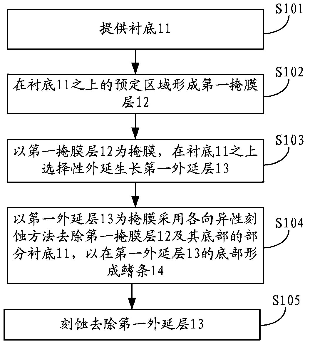
[0088] figure 1 It shows a schematic flow chart of the method for manufacturing semiconductor fins according to an embodiment of the present invention. Figures 2a(1) to 2d(2) show the structural schematic diagrams of semiconductor fins at various stages in the production process, where Figure (1) is Top view, Figure (2) is the cross-sectional view of Figure (1) along the AA' direction, combined together figure 1 ~ Figure 2d (2), the process of the manufacturing method of the semiconductor fins is as follows:
[0089] S101 , providing a substrate 11 , as shown in FIGS. 2 a ( 1 ) and 2 a ( 2 ).
[0090] The substrate 11 in Embodiment 1 of the present invention is a bulk silicon substrate. The bulk silicon substrate may be a P-well substrate, an N-well substrate or a double-well substrate.
[0091] S102: Forming a first mask layer 12 in a predetermined area on the substrate 11, as shown in FIGS. 2b(1) and 2b(2).
[0092] The first mask layer 12 can be fabricated by a selectiv...
Embodiment 2
[0107] image 3 A schematic flow chart showing a method for manufacturing semiconductor fins according to an embodiment of the present invention, Figure 4a ~ Figure 4i Schematic diagrams showing the structure of semiconductor fins at various stages in the fabrication process, together with Figure 3 ~ Figure 4i , the process flow of the manufacturing method of the semiconductor fins is as follows:
[0108] In view of the fact that S301-S305 are the same as or corresponding to S101-S105 in the above embodiment, correspondingly, Figure 4a ~ Figure 4e It is the same as or corresponding to FIG. 2 a ( 2 ) to FIG. 2 d ( 2 ), and will not be repeated here. For details, refer to the relevant description in the foregoing embodiments.
[0109] S306, forming side walls 15 on both sides of the fin ray 14, such as Figure 4f shown.
[0110]The sidewalls 15 are formed on both sides of the fin 14 by a combination of deposition and etch-back. For example, one or more layers of material...
Embodiment 3
[0121] Figure 5 It shows a schematic flow chart of the manufacturing method of the FinFET device according to the embodiment of the present invention, wherein the FinFET device adopts the semiconductor fin strips manufactured by the manufacturing method described in the above embodiment. Figures 6a(1)-6l(3) show the Schematic diagram of the structure of FinFET devices at various stages, where Figure (1) is a top view, Figure (2) is a cross-sectional view of Figure (1) along the AA' direction, and Figure (3) is a cross-sectional view of Figure (1) along the BB' direction . combined Figure 5 ~ Figure 6l (3), the process of the manufacturing method of the FinFET device is as follows:
[0122] S501 , providing a substrate 11 , as shown in FIGS. 6 a ( 1 ) and 6 a ( 2 ).
[0123] In the embodiment of the present invention, the substrate 11 is a bulk silicon substrate. The bulk silicon substrate may be a P-well substrate, an N-well substrate or a double-well substrate.
[0124...
PUM
 Abstract
Description
Claims
Application Information
 - R&D
- Intellectual Property
- Life Sciences
- Materials
- Tech Scout
- Unparalleled Data Quality
- Higher Quality Content
- 60% Fewer Hallucinations
Browse by: Latest US Patents, China's latest patents, Technical Efficacy Thesaurus, Application Domain, Technology Topic, Popular Technical Reports.
© 2025 PatSnap. All rights reserved.Legal|Privacy policy|Modern Slavery Act Transparency Statement|Sitemap|About US| Contact US: help@patsnap.com