Semi-distributed passive variable attenuator

A distributed attenuation and semi-distributed technology, applied in the field of electronics, can solve the problems of increasing the manufacturing cost of the attenuator, increasing the circuit complexity, and being unable to process and manufacture, and achieving good port matching characteristics, simple structure, and low signal power loss. Effect

Active Publication Date: 2013-12-04
XIDIAN UNIV
View PDF4 Cites 22 Cited by
  • Summary
  • Abstract
  • Description
  • Claims
  • Application Information

AI Technical Summary

Problems solved by technology

However, the disadvantage of this patented technology is that the phase compensation structure increases the complexity of the circuit and is not suitable for integrated systems
The disadvantage of the attenuator system disclosed in this patent technology is that the variable attenuator system, as the PIN diode of the control switch, cannot be directly processed and manufactured by the existing large-scale integrated circuit manufacturing process, and additional process steps are required for manufacture. , increasing the manufacturing cost of the attenuator

Method used


Image

  • Semi-distributed passive variable attenuator
  • Semi-distributed passive variable attenuator
  • Semi-distributed passive variable attenuator

Examples


Embodiment 1

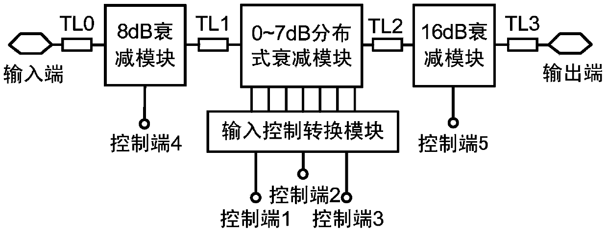
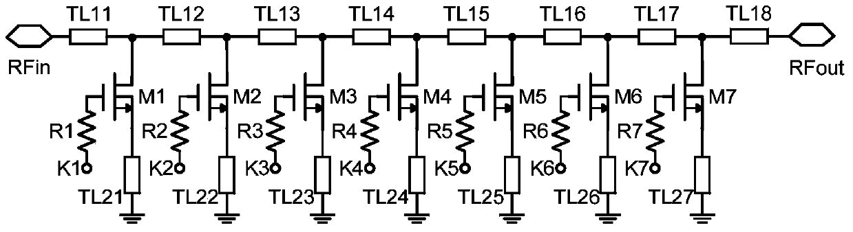
[0063] Example 1: Combining figure 1 , figure 2 , Embodiment 1 of the present invention adopts microstrip line distributed hybrid T-π attenuation structure, with Figure 6 The field effect transistor switch with the body terminal connected to the source electrode as shown is used as the control switch of the parallel branch. The 0-7dB distributed attenuation module is jointly controlled by seven-digit digital signals at seven control ports K1, K2, K3, K4, K5, K6, and K7 to achieve 0-7dB attenuation with a step length of 1dB. The different level states of the input control signals of each control terminal and the corresponding signal amplitude attenuation states are shown in the table below. In the table, 0 means low level and 1 means high level.

[0064]

[0065] As can be seen from the above table, the 0-7dB distributed attenuation module of the present invention changes the high and low level state of the input control signal through seven control ports K1, K2, K3, K4...

Embodiment 2

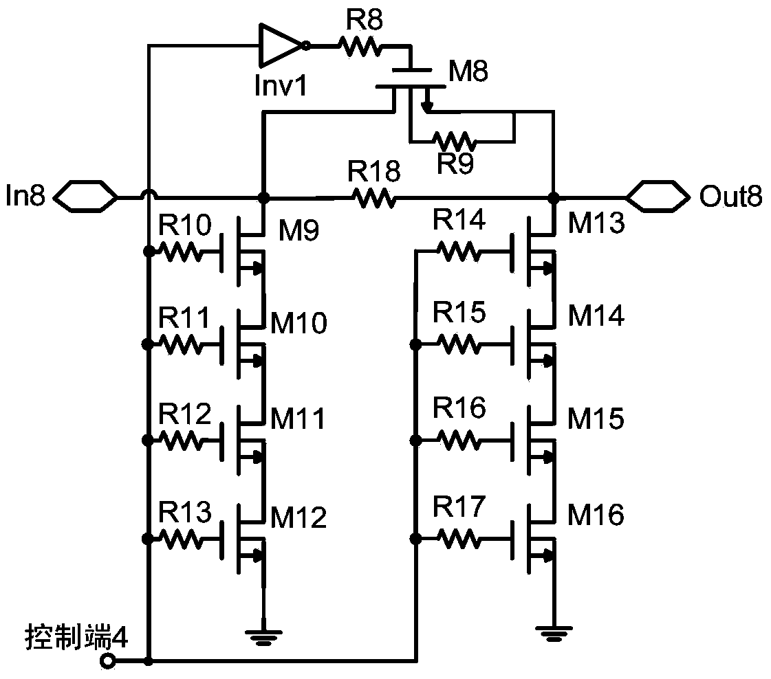
[0066] Example 2: Combining figure 1 , image 3 , Embodiment 2 of the present invention adopts a π-type attenuation structure to Figure 7 The field effect transistor with channel parallel resistance structure shown is used as the control switch of the series branch to Figure 8 The stacked field effect transistors shown serve as control switches for the parallel branches. The 8dB attenuation module performs attenuation control at the control terminal 4 by a digital signal. When the control terminal 4 is low level, the input of the inverter Inv1 is low level, the output of the inverter Inv1 is high level, the switch field effect transistor M8 is turned on, and the switch field effect transistors M9, M10, M11, M12, M13 , M14, M15 and M16 are all turned off, and the 8dB attenuation module is in the reference state. When the control terminal 4 is at a high level, the input of the inverter Inv1 is at a high level, the output of the inverter Inv1 is at a low level, the switchin...

Embodiment 3

[0067] Example 3: Binding figure 1 , Figure 4 , Embodiment 3 of the present invention adopts a π-type attenuation structure to Figure 7 The field effect transistor with channel parallel resistance structure shown is used as the control switch of the series branch to Figure 8 The stacked field effect transistors shown serve as control switches for the parallel branches. The 16dB attenuation module performs attenuation control at the control terminal 5 by a digital signal. When the control terminal 5 is low level, the input of the inverter Inv2 is low level, the output of the inverter Inv2 is high level, the switch field effect transistor M17 is turned on, and the switch field effect transistors M18, M19, M20, M21, M22 , M23, M24 and M25 are all turned off, and the 16dB attenuation module is in the reference state. When the control terminal 5 is at a high level, the input of the inverter Inv2 is at a high level, the output of the inverter Inv2 is at a low level, the switc...


PUM


Abstract

The invention discloses a semi-distributed passive variable attenuator. The semi-distributed passive variable attenuator comprises a 0-7dB distributed attenuation module, an 8dB attenuation module, a 16dB attenuation module and an input control conversion module. A switch field effect transistor adopting the structure that a body end is connected with a source electrode, a switch field effect transistor provided with a channel parallel connection resistor structure and a switch field effect transistor of a stacked structure are used as control switches. The semi-distributed passive variable attenuator is controlled by a five-digit figure signal to operate independently. Coplanar waveguide transmission lines are used for matching adjacent attenuation modules and matching 50-omega input impedance and 50-omega output impedance. The operating frequency range of the semi-distributed passive variable attenuator is 0-50 GHz, wherein the semi-distributed passive variable attenuator can realize 32 states of low-loss low-phase shift signal amplitude attenuation by stepping with the length of 1dB in the attenuation range of 0-31dB. The semi-distributed passive variable attenuator has the advantages of being low in loss and additional phase shift, high in degree of linearity, wide in operation frequency band, simple in circuit structure, and applicable to a radio frequency / microwave system processing high-power signals.

Description

technical field [0001] The invention belongs to the field of electronic technology, and further relates to a semi-distributed passive variable attenuator in the field of radio frequency / microwave communication system integrated circuit technology. The invention can be used as a functional module for achieving low differential loss variable gain attenuation for signal amplitude in ultra-wideband radio frequency / microwave communication systems, automatic gain control systems, phased array systems, and electronic countermeasure systems. Background technique [0002] At present, in the field of radio frequency / microwave communication system integrated circuit technology, variable attenuators are widely used in ultra-wideband radio frequency / microwave communication systems, automatic gain control systems, phased array systems, and electronic countermeasure systems to achieve low signal amplitude loss. Vary the gain reduction. The digital attenuator with small insertion phase var...

Claims


Application Information

Patent Timeline
Patent Type & Authority Applications(China)
IPC IPC(8): H03H7/24
Inventor 庄奕琪李振荣张岩龙靳刚汤华莲张丽李聪曾志斌
Owner XIDIAN UNIV
Why Eureka
Try Eureka