Scanning slit device used in stepping scan lithography machine

A step scanning and lithography technology, applied in the field of lithography, can solve the problems of different diffraction effects, inability to realize plane scanning motion, and no scanning function.

Active Publication Date: 2015-03-25
BEIJING GUOWANG OPTICAL TECH CO LTD
View PDF5 Cites 0 Cited by
  • Summary
  • Abstract
  • Description
  • Claims
  • Application Information

AI Technical Summary

Problems solved by technology

However, the biggest problem with this method is that it cannot meet the two requirements of scanning in any range in the plane and scanning in two dimensions.
If it is necessary to scan in any range within the plane, the scanning blades in the two-dimensional direction need to be separated from a certain distance in the direction of the optical axis to avoid interference with each other, so that the slit surface, the mask surface and the silicon wafer in the optical path The ideal conjugate relationship cannot be formed between the surfaces, and the diffraction effects formed by the knife edges in the two directions are also different, which affects the uniformity of the exposure dose; if the knife edges in the two-dimensional directions require coplanarity, only one of them can be selected. One dimension has a scanning function, and the other dimension can only be designed as a fixed opening with a suitable size, but does not have a scanning function. Therefore, this scanning slit cannot realize any range of scanning motion in the plane.

Method used


Image

  • Scanning slit device used in stepping scan lithography machine
  • Scanning slit device used in stepping scan lithography machine
  • Scanning slit device used in stepping scan lithography machine

Examples


Embodiment Construction

[0022] Below in conjunction with accompanying drawing and specific implementation example, the present invention is described in detail:

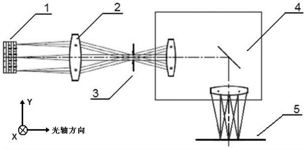
[0023] see figure 2 , figure 2 It is a schematic diagram of a part of the optical path of an exposure system including a scanning slit device for a step-and-scan lithography machine according to the present invention. The illuminating light beam from the front end passes through the homogenizing element 1 and converges on the knife-edge surface of the scanning slit 3 through the condenser lens group 2 . The knife-edge surface of the scanning slit 3 is perpendicular to the optical axis, and the outline of the field of view formed by the knife-edge surface is projected onto the mask surface 5 through the illumination mirror group 4 .

[0024] In this implementation example, if figure 2 As shown, two directions perpendicular to each other are set on the knife-edge surface of the scanning slit 3, wherein the direction perpendicular to the...


PUM


Abstract

A scanning slit device used in a stepping scan lithography machine is formed by connecting four identical blade components through four limit connecting pieces, the four limit connecting pieces are used for closely connecting every two adjacent blade components, four blade components are integrated in two orthogonal directions according to a rotary and symmetrical manner, knife edges of the adjacent blade components are mutually perpendicular to each other, four knife edges are coplanar and perpendicular to an optical axis of a system, and openings formed between the four knife edges are scanning slits. The invention not only can realize high-precision two-dimensional scanning at an optional plane range in a maximum stroke, but also can ensure coplanarity of the scanning knife edges in the two-dimensional directions.

Description

technical field [0001] The invention relates to a photolithography machine, in particular to a scanning slit device for a step-and-scan photolithography machine. The light blocking device of semiconductor equipment, especially the scanning slit device in the exposure system of a lithography machine that keeps moving synchronously with the mask / silicon wafer stage. technical background [0002] The production of large-scale integrated circuits is the core of modern microelectronics technology, and semiconductor equipment is the basis for the development of integrated circuits. In the current semiconductor manufacturing equipment, lithography equipment occupies the most important position. After the lithography technology has experienced several major technical development stages of proximity / contact, scanning projection, and step projection, step and scan projection has developed into the current mainstream technology. [0003] The step-and-scan projection lithography machi...

Claims


Application Information

Patent Timeline
Patent Type & Authority Patents(China)
IPC IPC(8): G03F7/20
Inventor 林栋梁马兴华任冰强程伟林张友宝钱珍梅屈建峰孙征宇黄惠杰
Owner BEIJING GUOWANG OPTICAL TECH CO LTD
Why Eureka
Try Eureka