Band-gap reference voltage source structure without passive elements based on standard CMOS technology

A technology of reference voltage source and passive components, applied in the direction of regulating electrical variables, control/regulating systems, instruments, etc., can solve problems such as unfavorable integration design and cost control, achieve good versatility and reduce the effect of offset voltage

Active Publication Date: 2013-12-11
中科芯未来微电子科技成都有限公司
View PDF6 Cites 5 Cited by
  • Summary
  • Abstract
  • Description
  • Claims
  • Application Information

AI Technical Summary

Problems solved by technology

However, the existing problems are also obvious. For example, many solutions have special processes to improve performance, and the core circuit and operational amplifier circuit often contain actual resistance and capacitance components, which are not conducive to further integrated design and cost. control

Method used


Image

  • Band-gap reference voltage source structure without passive elements based on standard CMOS technology

Examples


Embodiment Construction

[0015] The present invention will be further described below in conjunction with drawings and embodiments.

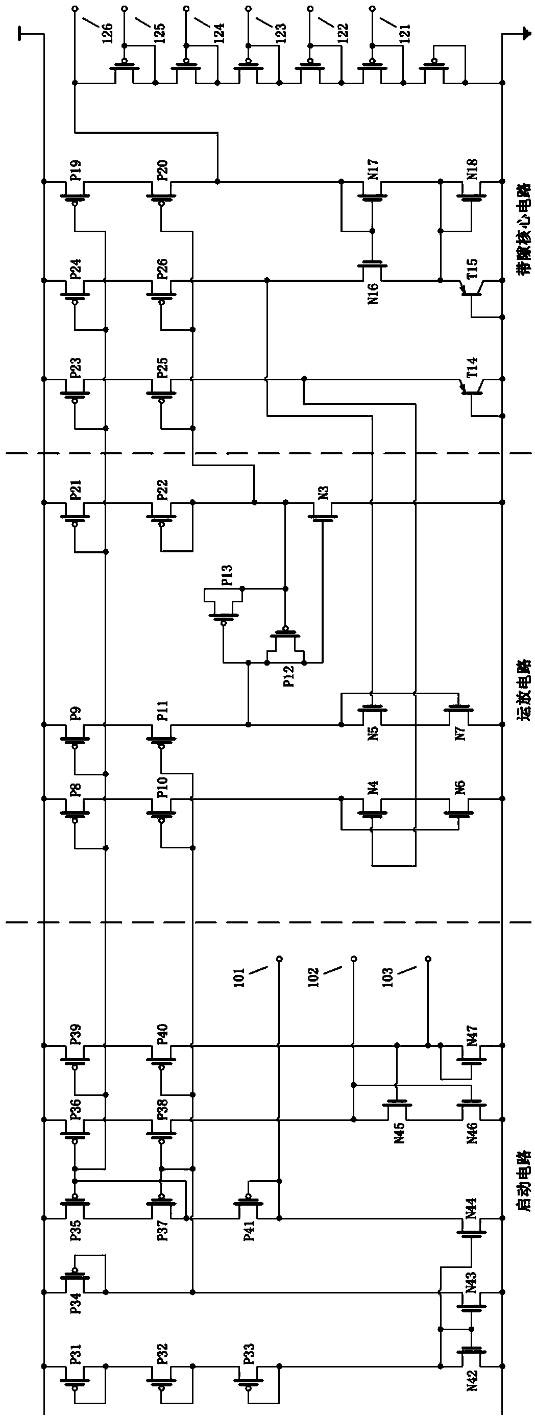
[0016] Such as figure 1 As shown, the bandgap reference voltage source of the present invention is composed of three parts, namely a start-up circuit, an operational amplifier circuit and a bandgap core circuit. The output bias terminal of the start-up circuit is connected to the gate bias terminal of the current mirror of the op-amp circuit and the bandgap core circuit, and the start-up circuit makes the subsequently connected op-amp circuit and the bandgap core circuit work in a suitable state through a stable voltage bias point. The static operating point thus starts the whole circuit; the tail current NMOS tube of the primary circuit of the op amp circuit is connected to the drain of the input NMOS tube of the same branch, and the Miller compensation PMOS tube between the secondary circuit and the primary circuit is connected head-to-tail. That is, any PMOS transis...


PUM


Abstract

The invention relates to a band-gap reference voltage source structure which is mainly designed for reaching the strict standard CMOS technology and not comprising passive elements. A starting circuit is characterized by having good generality. The key point of an operational amplifying circuit is that an optimization design and a Miller compensation design are performed on reduction of offset voltage, wherein the Miller compensation design is that a common-mode feedback structure of tail current discrete pair tubes and MOS pair tubes are used for replacing traditional resistive and capacitive components. According to a band-gap core circuit, in order to achieve the purpose of removing the passive elements, a linear region MOS tube is used for replacing a polycrystalline silicon resistor, and meanwhile current mirror sub-circuit MOS tubes at the output end are optimized in order to obtain reference voltage based on other principles and keep a longitudinal PNP pair tube design in the standard CMOS technology. In addition, on the basis of the obtained band-gap reference voltage, a serial structure of MOS tubes is flexibly configured, therefore, reference points of equally divided voltage and specified voltage can be obtained, and for a band-gap reference source often used in a data conversion circuit and a storage circuit, the reference points have excellent practical value.

Description

technical field [0001] The invention relates to a bandgap reference voltage source, in particular to a bandgap reference voltage source structure completely based on standard CMOS technology without any passive components. Background technique [0002] Bandgap references are widely used as basic and key devices in data conversion circuits and memory circuits. The current mainstream research trend of bandgap reference tends to pursue high precision at lower voltage and lower power consumption. However, the existing problems are also obvious. For example, many solutions have special processes to improve performance, and the core circuit and operational amplifier circuit often contain actual resistance and capacitance components, which are not conducive to further integrated design and cost. control. Contents of the invention [0003] The purpose of the present invention is to overcome the deficiencies in the prior art and provide a general bandgap reference voltage source ...

Claims


Application Information

Patent Timeline
Patent Type & Authority Applications(China)
IPC IPC(8): G05F1/56
Inventor 孙业超黄卓磊王玮冰
Owner 中科芯未来微电子科技成都有限公司
Why Eureka
Try Eureka