Semiconductor package piece and manufacturing method thereof

A manufacturing method and packaging technology, applied in semiconductor/solid-state device manufacturing, semiconductor devices, semiconductor/solid-state device components, etc., can solve problems such as insufficient bonding force and weak bonding, so as to increase the area of ​​the electroplating layer and ensure firmness performance, improve the effect of welding firmness

Inactive Publication Date: 2013-12-11
GREAT TEAM BACKEND FOUNDRY (DONGGUAN) LTD
View PDF5 Cites 5 Cited by
  • Summary
  • Abstract
  • Description
  • Claims
  • Application Information

AI Technical Summary

Problems solved by technology

Existing semiconductor packages are often combined with PCBs due to insufficient bonding force, resulting in weak bonding

Method used


Image

  • Semiconductor package piece and manufacturing method thereof
  • Semiconductor package piece and manufacturing method thereof
  • Semiconductor package piece and manufacturing method thereof

Examples


Embodiment 1

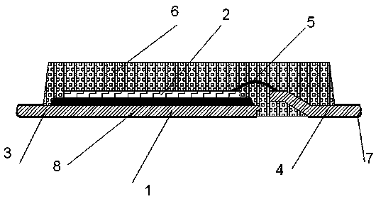
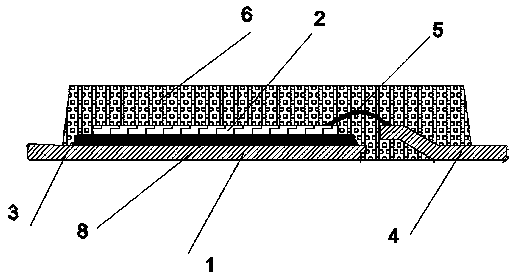
[0029] refer to figure 1 , a semiconductor package, comprising a lead frame 1 and a chip 2, the lead frame 1 has a chip holder 3, the chip 2 is fixed on the chip holder 3 by a bonding material 8, the chip 2 and the lead frame The pin 4 of 1 is connected with a welding wire 5, and an encapsulation compound 6 covers the chip 2 on the lead frame 1. The exposed part of the lead frame 1 is plated with an electroplating layer 7, and at the same time, the side of the pin 4 of the lead frame is plated with Tin layer 7.

[0030] In this embodiment, the tin-plated layer 7 is plated on the exposed part of the lead frame 1, especially the tin-plated layer 7 is plated on the side of the lead frame pin 4, so as to increase the tin-plated layer and the area of ​​the tin-plated layer of the lead frame 1, Therefore, when the semiconductor package is subsequently welded to the PCB board, the firmness of welding of the two is improved.

Embodiment 2

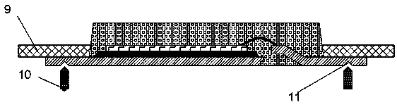
[0032] refer to figure 2 , image 3 , Figure 6 and Figure 7 , a method for manufacturing a semiconductor package, the method steps comprising:

[0033] s1, lay the lead frame 1 flat, and then fix the chip 2 on the chip holder 3 of the lead frame 1 through the bonding material 8, the chip 2 and the pin 4 of the lead frame 1 are connected with a bonding wire 5, and an encapsulation compound 6 Covering the chip 2 on the lead frame 1;

[0034] s2, the inherent concave template 9 on the lead frame 1, use the punch 10 to half-cut the bottom of the two sides of the lead frame 1 (specifically, the chip holder 3 and the pin 4), and the two sides of the lead frame 1 (specifically, the chip holder) 3 and pin 4) Dig out a "∧" shaped gap 11 at the bottom;

[0035] s3, electroplating and tinning the lead frame 1 with the notch 11 dug out in s2, and plating the tin-plated layer 7 on the external exposed part of the lead frame 1;

[0036] s4, the inherent concave template on the lead...


PUM


Abstract

The invention discloses a semiconductor package piece and a manufacturing method thereof. The semiconductor package piece comprises a lead frame and a chip, wherein an electroplated layer is plated at the exposed part of the lead frame, and an electroplated layer is plated on the side surface of the pin of the lead frame. According to the manufacturing method of the semiconductor package piece, before an electroplating process, a notch is made so as to increase the area of the electroplated layer on the side surface of the pin of the lead frame. As the electroplated layer is plated at the exposed part of the lead frame, and particularly, the electroplated layer is plated on the side surface of the pin of the lead frame, the semiconductor package piece and a PCB (printed circuit board) are guaranteed to be welded firmly in the following process of welding the semiconductor package piece onto the PCB. The semiconductor package piece manufactured by the manufacturing method and the PCB are guaranteed to be welded firmly in the following process of welding the semiconductor package piece onto the PCB.

Description

technical field [0001] The invention belongs to the field of semiconductor packages, and in particular relates to a semiconductor package and a manufacturing method thereof. Background technique [0002] As the chip carrier of integrated circuits, the lead frame is a key structural part that realizes the electrical connection between the lead-out end of the chip's internal circuit and the outer lead by means of a bonding material, forming an electrical circuit. It acts as a bridge connecting the external wire. Most semiconductor integrated blocks need to use lead frames, which are important basic materials in the electronic information industry. [0003] The existing semiconductor package that uses a lead frame as a semiconductor chip carrier is to connect the non-active surface of the semiconductor chip to the chip seat of the lead frame, and then electrically connect the active surface of the semiconductor chip to the tube of the lead frame through a plurality of bonding w...

Claims


Application Information

Patent Timeline
Patent Type & Authority Applications(China)
IPC IPC(8): H01L23/495H01L21/48
CPCH01L2224/32245H01L2224/48091H01L2224/48247H01L2224/73265H01L2924/00014H01L2924/00
Inventor 黄源炜徐振杰曹周敖利波
Owner GREAT TEAM BACKEND FOUNDRY (DONGGUAN) LTD
Why Eureka
Try Eureka