Atomic-order flat surface treatment method of silicon wafer, and heat treatment device

A heat treatment device and surface treatment technology, applied in the field of planarization treatment, can solve problems such as undisclosed crystalline defects, unmentioned mass production, etc., and achieve the effect of high yield

Inactive Publication Date: 2013-12-11
TOHOKU UNIV
View PDF1 Cites 5 Cited by
  • Summary
  • Abstract
  • Description
  • Claims
  • Application Information

AI Technical Summary

Problems solved by technology

[0013] However, according to the method of Patent Document 1, it is confirmed that even if a large-diameter silicon wafer such as 200mmφ is heat-treated at a low temperature of 850°C in an atmosphere of high-purity Ar gas, the so-called slip line does not form. Crystalline defects, however, Patent Document 1 does not mention whether it is suitable for mass production, whether it

Method used


Image

  • Atomic-order flat surface treatment method of silicon wafer, and heat treatment device
  • Atomic-order flat surface treatment method of silicon wafer, and heat treatment device
  • Atomic-order flat surface treatment method of silicon wafer, and heat treatment device

Examples


Embodiment 1

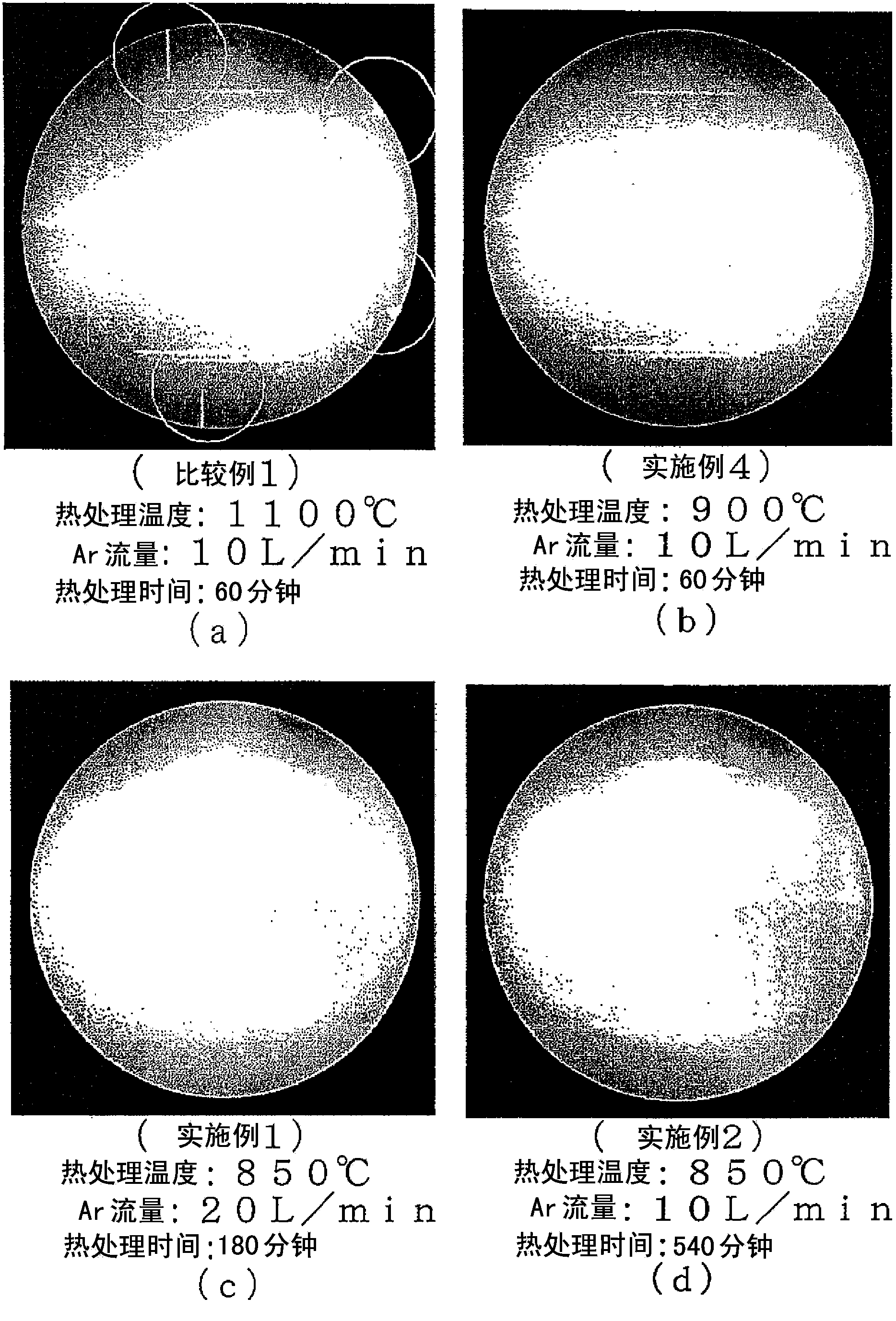
[0104] First, a silicon wafer with a diameter of 200mmφ and (100) orientation on the surface was prepared, and the surface of the silicon wafer was cleaned according to the following steps. First, use the O 3 water, the silicon wafer surface was washed for 10 minutes, washed with dilute HF (0.5 wt%) for 1 minute, and finally rinsed with ultrapure water for 3 minutes.

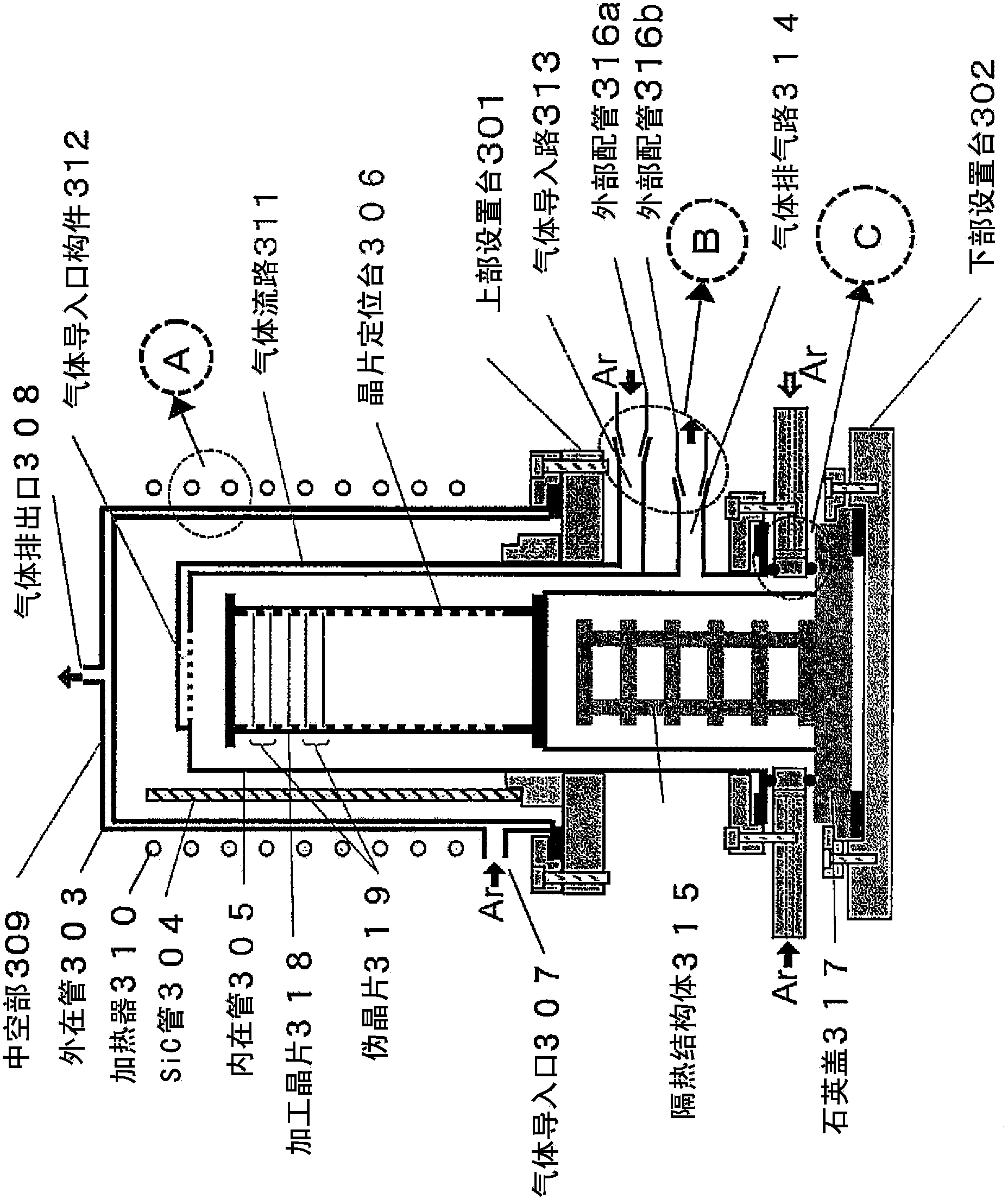
[0105] Then, in image 3 The silicon wafer is placed in the heat treatment apparatus shown, and the water flowing in at 20L / min is 0.2ppb or less, O 2 Heat treatment was performed at a heat treatment temperature of 850° C. and a heat treatment time of 180 minutes while Ar was 0.1 ppb or less.

[0106] However, during heat treatment, do not follow the Figure 4 , 5 , 6 to implement, and set to the above-mentioned patent document 1 Figure 9 Conditions of the heat treatment apparatus equivalent to those carried out in the heat treatment apparatus described in .

[0107] Specifically, first, according to Fi...

Embodiment 2

[0109] A sample was prepared under the same conditions as in Example 1 except that the Ar flow rate was 10 L / min and the heat treatment time (holding time) was 540 minutes.

Embodiment 3

[0111] A sample was prepared under the same conditions as in Example 1 except that the Ar flow rate was 10 L / min and the heat treatment time (holding time) was 270 minutes.


PUM


Abstract

Disclosed is a silicon wafer wherein a plurality of terraces are formed on the surface with steps which are formed of a monatomic layer. There is no slip line in the wafer.

Description

technical field [0001] The invention relates to a planarization treatment method for the surface of a silicon wafer used for making semiconductor devices such as IC and LSI. Background technique [0002] The irregularities on the surface of silicon wafers used to make semiconductor devices such as ICs and LSIs hinder the improvement of the current drive capability of MOSFETs (Metal Oxide Semiconductor Field Effect Transistors) as shown in Non-Patent Document 1, for example. The main reason is that the surface is required to be planarized as much as possible. [0003] On the other hand, it has been reported that when a silicon wafer is heat-treated in an Ar environment at 1200° C., an ultimate flat surface exhibiting atomic-level step and terrace structures can be formed (Non-Patent Document 2). [0004] However, it is unrealistic to consider mass production under high-temperature treatment such as 1200°C. [0005] On the other hand, Patent Document 1 describes that by perf...

Claims


Application Information

Patent Timeline
IPC IPC(8): H01L21/324H01L21/02H01L21/302
CPCH01L21/02052H01L21/02236H01L21/02252H01L21/3247H01L21/67017H01L21/67757H01L29/045H01L21/02H01L21/324
Inventor 大见忠弘寺本章伸诹访智之
Owner TOHOKU UNIV
Why Eureka
Try Eureka