Electrostatic chuck device

An electrostatic chuck and electrostatic adsorption technology, applied in the direction of circuits, electrical components, sleeve/socket connections, etc., can solve problems such as differences in chip temperature distribution, ease stress and thermal expansion differences, reduce the generation of voids, and softness excellent effect

Active Publication Date: 2013-12-11
SUMITOMO OSAKA CEMENT CO LTD
View PDF9 Cites 5 Cited by
  • Summary
  • Abstract
  • Description
  • Claims
  • Application Information

AI Technical Summary

Problems solved by technology

In addition, the in-plane temperature distribution of the wafer is di

Method used


Image

  • Electrostatic chuck device

Examples


Embodiment

[0099] Hereinafter, although an Example and a comparative example demonstrate this invention concretely, this invention is not limited to these Examples.

[0100] {Example}

[0101] (Fabrication of electrostatic chuck device)

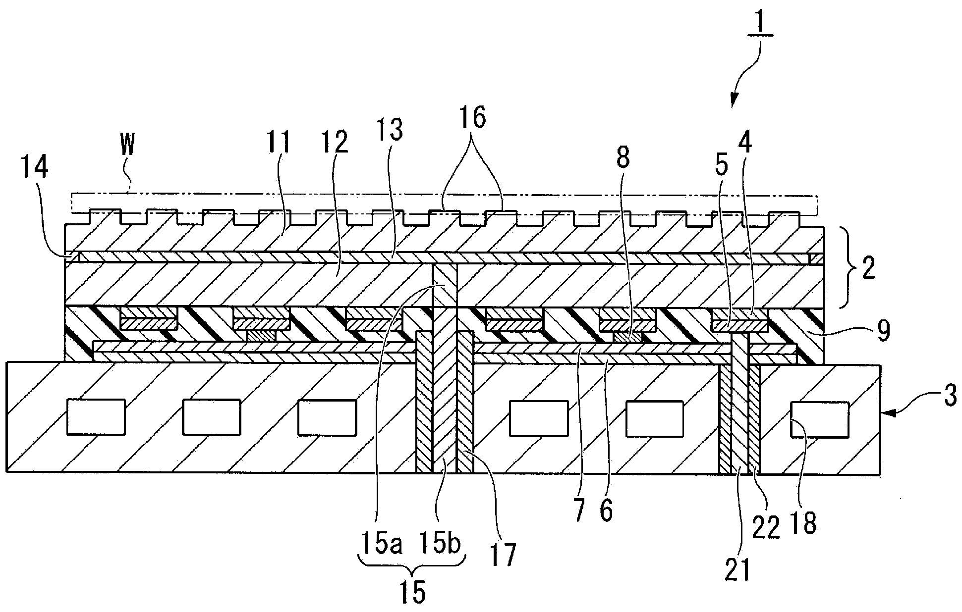
[0102] The electrostatic chuck portion 2 in which the internal electrode 13 for electrostatic adsorption with a thickness of 15 μm was embedded was produced by a known method. The mounting plate 11 of the electrostatic chuck unit 2 is an alumina-silicon carbide composite sintered body containing 8% by mass of silicon carbide, and has a disc shape with a diameter of 320 mm and a thickness of 4 mm.

[0103] In addition, the supporting plate 12 is also an alumina-silicon carbide composite sintered body containing 8% by mass of silicon carbide similarly to the placing plate 11 , and has a disc shape with a diameter of 320 mm and a thickness of 4 mm. The overall thickness of the electrostatic chuck unit 2 was set to 8 mm by joining and integrating the abov...


PUM

PropertyMeasurementUnit
Thicknessaaaaaaaaaa

Abstract

This electrostatic chuck device (1) comprises an electrostatic chuck part (2), which has one primary surface as a supporting surface for supporting plate-shaped samples and in which internal electrodes for electrostatic adsorption are housed, and a cooling base part (3) for cooling the electrostatic chuck part (2), wherein a heating member (5) is adhered, via a first adhesive member layer (4), to the other primary surface of the electrostatic chuck part (2) on the side opposite the supporting surface; the electrostatic chuck part (2) and heating member (5), and the cooling base part (3) are integrally adhered via an acrylic adhesive agent layer (9) having flexibility and insulating properties performance.

Description

technical field [0001] The present invention relates to electrostatic chuck devices. More specifically, the present invention relates to an electrostatic chuck which is suitable for use in the etching process such as plasma etching in semiconductor manufacturing process and is not corroded by the gas used when attaching and fixing a plate-shaped sample such as a semiconductor wafer by electrostatic force. device. [0002] this application claims priority based on Japanese Patent Application No. 2011-064311 for which it applied to Japan on March 23, 2011, The content is used for this specification. Background technique [0003] In recent years, in semiconductor manufacturing processes, further improvement in microfabrication technology has been demanded along with higher integration and higher performance of devices. In this semiconductor manufacturing process, etching technology is also an important microfabrication technology. In recent years, among etching technologies, ...

Claims


Application Information

Patent Timeline
IPC IPC(8): H01L21/683
CPCH01L21/67109H01L21/6831Y10T279/23H01L21/683H01L21/6833
Inventor 三浦幸夫前田进一佐藤隆古内圭
Owner SUMITOMO OSAKA CEMENT CO LTD
Why Eureka
Try Eureka