Late in-situ doped silicon germanium bonding for pmos devices
A silicon germanium and silicon nitride technology, applied in the field of ultra-low power technology, can solve problems such as lack of performance and low hole mobility
- Summary
- Abstract
- Description
- Claims
- Application Information
AI Technical Summary
Problems solved by technology
Method used
Image
Examples
Embodiment Construction
[0019] In the following description, for purposes of explanation, various specific details are set forth in order to provide a thorough understanding of the exemplary embodiments. It may be evident, however, that the exemplary embodiments may be practiced without these specific details, or with an equivalent arrangement. In other instances, well-known structures and devices are shown in block diagram representation in order to avoid unnecessarily obscuring the exemplary embodiments. In addition, unless otherwise specified, it should be understood that all numerals used in the specification and drawings represent numerical properties of quantities, ratios, components, reaction conditions, and the like. In all instances, the term "about" can be modified.
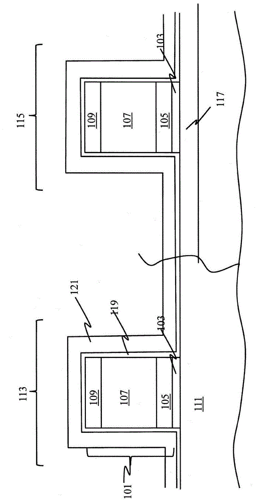
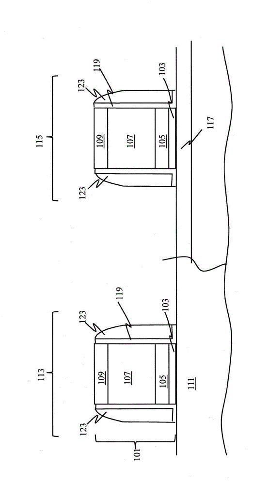
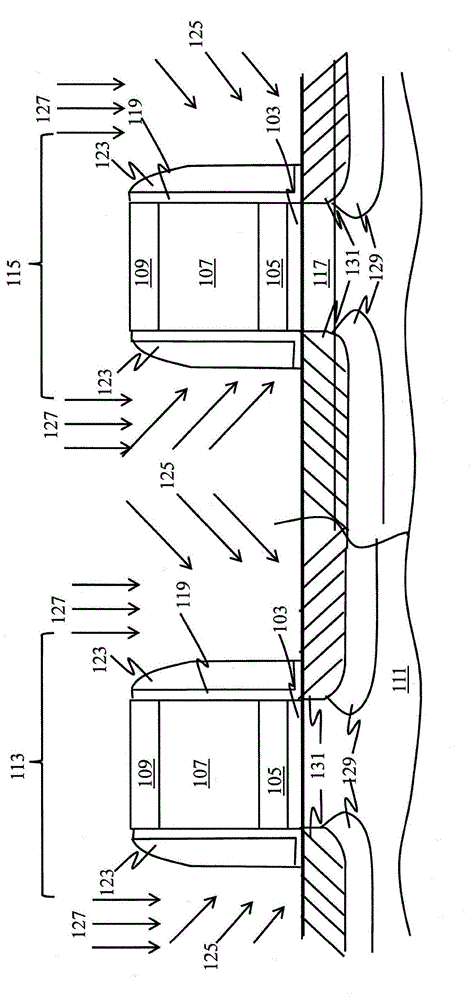
[0020] The present invention addresses and solves the current problem of insufficient cladding of gate first HKMG with the formation of embedded SiGe source / drain regions in PMOS devices. According to the disclosed embodimen...
PUM
 Abstract
Description
Claims
Application Information
 - R&D Engineer
- R&D Manager
- IP Professional
- Industry Leading Data Capabilities
- Powerful AI technology
- Patent DNA Extraction
Browse by: Latest US Patents, China's latest patents, Technical Efficacy Thesaurus, Application Domain, Technology Topic, Popular Technical Reports.
© 2024 PatSnap. All rights reserved.Legal|Privacy policy|Modern Slavery Act Transparency Statement|Sitemap|About US| Contact US: help@patsnap.com


