Supercharge Your Innovation With Domain-Expert AI Agents!

Interferometer for tsv detection and detection method using the interferometer

An interferometer, detection object technology, applied in semiconductor/solid-state device testing/measurement, instruments, measurement devices, etc., can solve the problems of less light quantity, large result data capacity, long detection time, etc.

Inactive Publication Date: 2016-01-06
SNU PRECISION CO LTD
View PDF6 Cites 0 Cited by
  • Summary
  • Abstract
  • Description
  • Claims
  • Application Information

AI Technical Summary

Problems solved by technology

[0003] The concept of three-dimensional structure has been applied in the field of packaging, but in the conventional method, since various terminals are arranged only on one side of the semiconductor chip and the signal terminals of multiple chips are electrically connected by soldering, the size of the chip and the layout of the wiring are limited. Issues arise in terms of complexity and power consumption
[0017] However, in conventional interferometers, when the lens that emits light toward the TSV is a wide-angle lens, the incident angle of the light entering the TSV is larger than the diameter of the through hole, so the amount of light entering the TSV is substantially small, and the light cannot reach the TSV. bottom surface
Therefore, it is virtually impossible to detect TSV
[0018] Moreover, even if the light source is replaced to further enhance the intensity of light reaching the bottom surface, it is necessary to detect the focal point of the light emitted to the TSV at a predetermined distance in the direction in which the TSV is formed, so the detection time is long, and the resulting data volume is large. The entire system generates overload problems

Method used


Image

  • Interferometer for tsv detection and detection method using the interferometer
  • Interferometer for tsv detection and detection method using the interferometer
  • Interferometer for tsv detection and detection method using the interferometer

Examples


experiment example 1

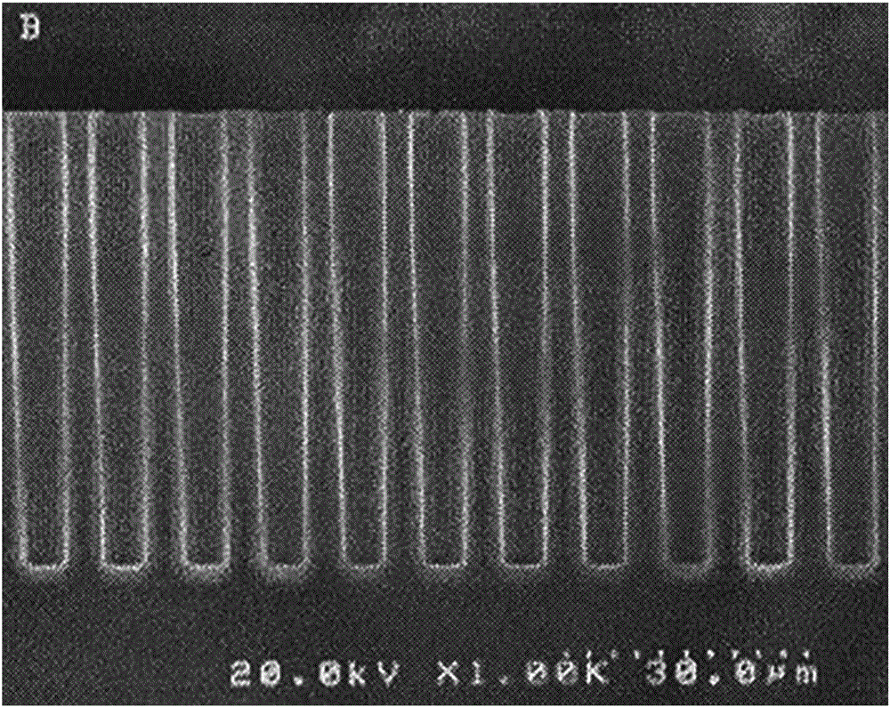
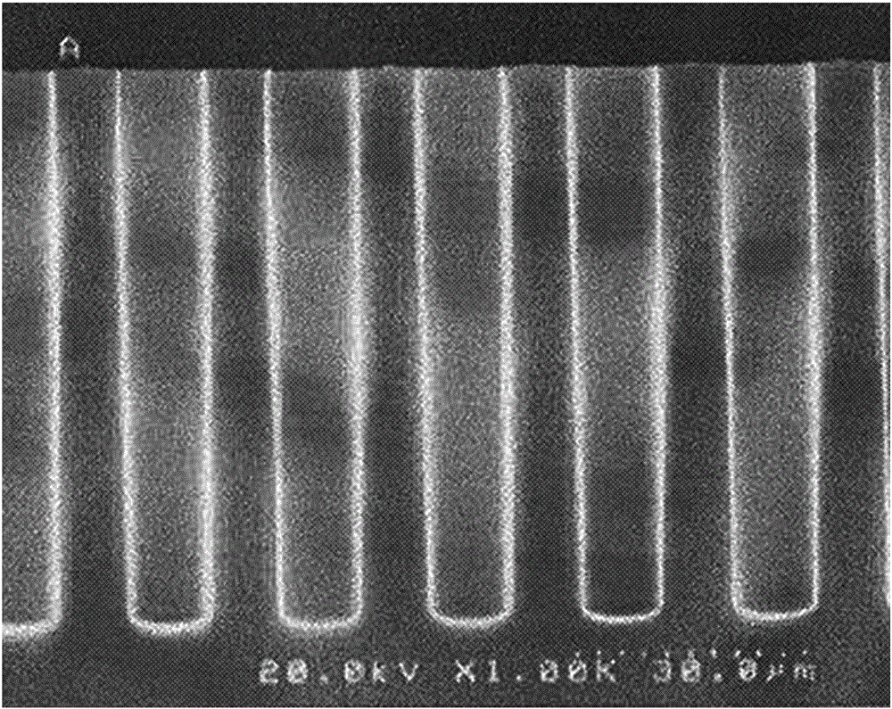
[0062] Prepare the substrate with TSVs, and use a conventional scanning electron microscope to obtain images such as Figure 5 SEM (Scanning Electron Microscope, scanning electron microscope) image, and directly measure (measured) the diameter and depth of TSV according to the SEM image.

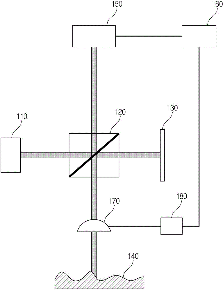
[0063] And, by figure 1 A conventional interferometer using a piezoelectric sensor divides the TSV into predetermined sections and performs continuous scanning to detect the diameter and depth of the TSV.

[0064] Moreover, the focal point is adjusted to the entrance of the TSV, that is, the reference position (TopCD) by the variable field diaphragm 80 of the TSV detection interferometer of the present invention and the first interference signal is acquired, and the variable field diaphragm 80 makes the The focus is adjusted to the bottom surface of the TSV, i.e. the variable position (BottomCD), and the second interference signal is acquired, and the diameter and depth of the TSV are detec...

experiment example 2

[0075] A substrate having a TSV having a shape different from that of Experimental Example 1 was prepared, and the experiment was carried out by the same method as Experimental Example 1 and obtained as follows: Figure 6 SEM image and measured TSV, using such as figure 1 The conventional interferometer and the interferometer for TSV detection of the present invention detect TSVs and acquire the following detection values.

[0076] [Table 2]

[0077]

Top CD(μm)

Bottom CD(μm)

Height(μm)

Measured value of SEM image

11

10

65

Detection value of conventional interferometer

11.0862

6.2675

-53.4829

Detection value of the interferometer of the present invention

11.1556

10.1995

-64.5011

[0078] As in Experimental Example 1, in Experimental Example 2, a value closer to the actual measured value was detected, which indicates that the detected value is more accurate as the diameter of the TSV increas...


PUM


Abstract

The invention relates to an interferometer for TSV detection and a detection method using the interferometer. The interferometer for TSV detection of the present invention uses a variable field diaphragm to detect the diameter and depth of a TSV when detecting a TSV, thereby shortening the detection time. time, and reduce the resulting data volume, where the iris diaphragm adjusts the focus of light to the entrance and bottom surface of the TSV. Furthermore, the present invention can ensure the amount of light reaching the bottom surface even when the aspect ratio is large like TSV by using a telecentric lens that makes the light incident on the TSV substantially linear.

Description

technical field [0001] The present invention relates to an interferometer for TSV detection and a detection method utilizing the interferometer, and in more detail relates to a variable field of view diaphragm arranged in the interferometer, thereby being able to detect such as TSV ( An interferometer for TSV detection having a diameter and depth of a through hole with a large aspect ratio, such as ThroughSiliconVia, and a detection method using the interferometer. Background technique [0002] Recently, in the field of semiconductors, in order to overcome the limitation of two-dimensional miniaturization technology of a chip with a limited area, the development of a chip with a three-dimensional structure has been proposed as a countermeasure. [0003] The concept of three-dimensional structure has been applied in the field of packaging, but in the conventional method, since various terminals are arranged only on one side of the semiconductor chip and the signal terminals o...

Claims


Application Information

Patent Timeline
Patent Type & Authority Patents(China)
IPC IPC(8): H01L21/66
CPCG01B2210/56H01L22/12H01L2924/0002H01L2924/00H01L22/00G01B11/24
Inventor 李基勋申兴铉朴喜载
Owner SNU PRECISION CO LTD
Features
  • R&D
  • Intellectual Property
  • Life Sciences
  • Materials
  • Tech Scout
  • Unparalleled Data Quality
  • Higher Quality Content
  • 60% Fewer Hallucinations
Learn More