Silicon wafer processing device
A processing device and silicon wafer technology, applied in the direction of electrical components, semiconductor/solid-state device manufacturing, test sample preparation, etc., can solve problems such as low production efficiency and environmental pollution, improve production efficiency, improve product quality, and avoid The effect of human injury
- Summary
- Abstract
- Description
- Claims
- Application Information
AI Technical Summary
Problems solved by technology
Method used
Image

Examples
Embodiment Construction
[0025] The present invention will be described in detail below in combination with specific embodiments and multiple drawings.
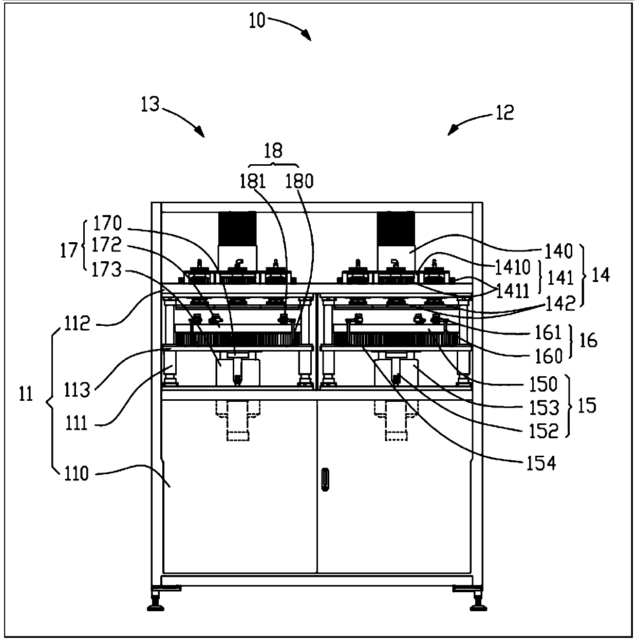
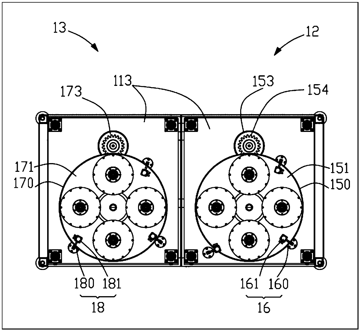
[0026] refer to figure 1 and figure 2 , the silicon wafer processing device 10 includes a machine platform 11 , a first processing part 12 and a second processing part 13 . The first processing part 12 and the second processing part 13 are sequentially arranged on the machine platform 11 .
[0027] The machine table 11 includes a base 110 , a pole 111 , an upper plate 112 and two moving plates 113 . The upper plate 112 is disposed above the base 110 through the pole 111 , and each moving plate 113 is located between the base 110 and the upper plate 112 and can move toward or away from the upper plate 112 .
[0028] The first processing unit 12 includes a silicon wafer mounting mechanism 14 , a first processing mechanism 15 and a first processing liquid supply mechanism 16 .
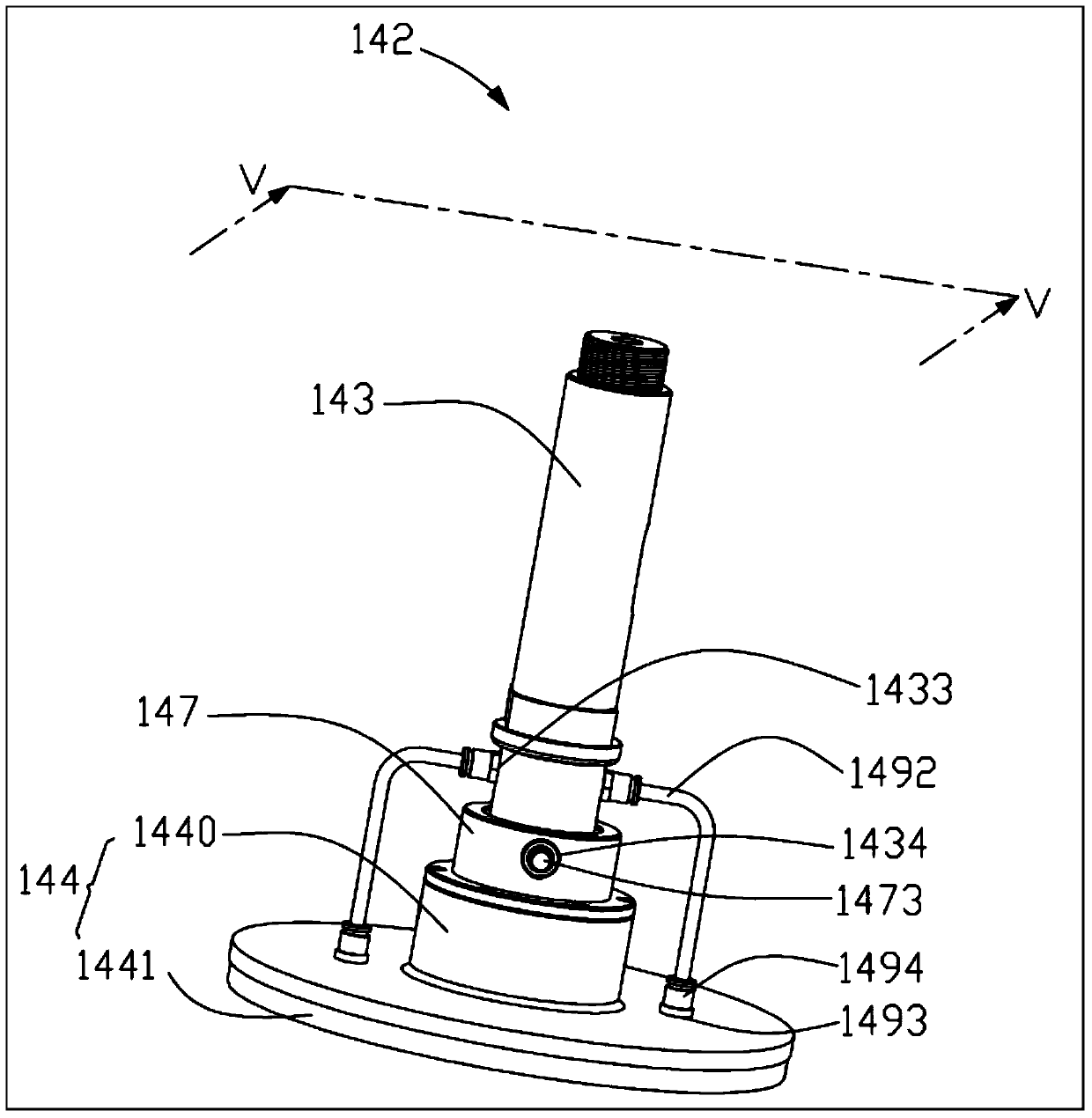
[0029] The wafer mounting mechanism 14 is disposed on the top of the m...
PUM
 Abstract
Description
Claims
Application Information
 - R&D
- Intellectual Property
- Life Sciences
- Materials
- Tech Scout
- Unparalleled Data Quality
- Higher Quality Content
- 60% Fewer Hallucinations
Browse by: Latest US Patents, China's latest patents, Technical Efficacy Thesaurus, Application Domain, Technology Topic, Popular Technical Reports.
© 2025 PatSnap. All rights reserved.Legal|Privacy policy|Modern Slavery Act Transparency Statement|Sitemap|About US| Contact US: help@patsnap.com