Manufacturing method of thin film transistor

A technology of thin-film transistors and manufacturing methods, applied in the field of microelectronics, capable of solving problems such as TFT device hysteresis, high defect density, and TFT performance degradation

Inactive Publication Date: 2013-12-25
SHANGHAI UNIV
View PDF3 Cites 14 Cited by
  • Summary
  • Abstract
  • Description
  • Claims
  • Application Information

AI Technical Summary

Problems solved by technology

But due to HfO 2 The defect density is very large, which will cause serious hysteresis in the manufactured TFT device, which will seriously degrade the performance of the TFT

Method used


Image

  • Manufacturing method of thin film transistor

Examples


Embodiment Construction

[0019] Embodiments of the present invention will be described in detail below in conjunction with the accompanying drawings.

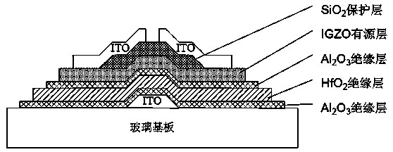
[0020] Such as figure 1 As shown, a method for manufacturing a thin film transistor has the following steps:

[0021] 1) Cleaning of the glass substrate: ultrasonically clean the glass in acetone, ethanol and deionized water for half an hour each to obtain a clean substrate;

[0022] 2) The ITO gate was prepared on the substrate by DC magnetron sputtering, and the sputtering conditions were: the background vacuum was 1.0×10 4 Pa, the gas pressure during sputtering is 0.7Pa, the flow rate of argon gas is 40sccm, the flow rate of oxygen gas is 0.5sccm, and the resistivity of the prepared ITO is 6.2×10 -4 Ω·cm, light transmittance above 80%. The thickness of the prepared film is 100nm, and the prepared film is glued, baked, photolithography, developed, etched and degummed to form an ITO electrode;

[0023] 3) Preparation of the first layer of Al 2 o ...


PUM


Abstract

The invention provides a manufacturing method of a thin film transistor. The thin film transistor is of a bottom grid structure and comprises a grid electrode, three insulating layers, an IGZO active layer, a SiO2 protection layer, a source electrode and a drain electrode, wherein the bottom is a glass substrate, the grid electrode ITO is deposited on the upper portion center area of the substrate with a magnetron sputtering method, the three insulating layers cover the grid electrode, the HfO2 insulating layer is in the middle, the Al2O3 insulating layers are on the two sides, a sandwich structure is formed by the HfO2 insulating layer and the Al2O3 insulating layers, Al2O3 and HfO2 are respectively prepared with the DC magnetron sputtering method and the sol gel method, the IGZO active layer and the SiO2 protection layer are sequentially arranged on the upper portion of the insulating layers, and the two ends of the source electrode and the two ends of the drain electrode are respectively located on the protection layer and the active layer.

Description

technical field [0001] The invention belongs to the technical field of microelectronics and relates to a manufacturing method of a thin film transistor. Background technique [0002] Over the past 20 years, Flat Panel Display (FPD) has developed rapidly, and its industrial scale has continued to expand. As early as 2002, the sales of flat panel display products have exceeded the sales of traditional CRT products. According to relevant statistics, in 2008, the output value of the world's flat panel display reached 103.4 billion US dollars, and this figure is expected to reach 111.8 billion US dollars in 2016. [0003] Thin-film transistors are widely used in the field of flat-panel displays as switches and driving elements. With the continuous development of AM-OLED and the demand for flexible display technology, people need TFT insulating layer materials with high dielectric strength for environmental protection and energy saving. permittivity, such TFTs can be driven at a ...

Claims


Application Information

Patent Timeline
Patent Type & Authority Applications(China)
IPC IPC(8): H01L21/336H01L21/28H01L29/786H01L29/51
Inventor 朱乐永李喜峰张建华
Owner SHANGHAI UNIV
Why Eureka
Try Eureka