Microstrip waveguide double-probe transition structure

A technology of transition structure and microstrip probe, applied in waveguide, waveguide-type devices, circuits, etc., can solve the problems of limited connection form, low efficiency, complex structure of frequency multiplier, etc., to reduce cost and processing time, and easy to use Fast, the effect of improving isolation

Inactive Publication Date: 2013-12-25
UNIV OF ELECTRONICS SCI & TECH OF CHINA
View PDF7 Cites 22 Cited by
  • Summary
  • Abstract
  • Description
  • Claims
  • Application Information

AI Technical Summary

Problems solved by technology

In the design of the frequency multiplier, due to the high frequency of the millimeter wave band, the optional frequency doubling devices (such as: Schottky diodes, etc.) are often limited in connection forms, such as for specific transmission TEM mode or quasi-TEM mode microstrip The transmission structure cannot realize the balanced frequency multiplier diode access, on the one hand, the structure of the frequency multiplier becomes complicated; on the other hand, the output of non-target frequency signals cannot be suppressed, and the efficiency is low

Method used


Image

  • Microstrip waveguide double-probe transition structure
  • Microstrip waveguide double-probe transition structure
  • Microstrip waveguide double-probe transition structure

Examples


Embodiment Construction

[0025] In order to make the object, technical solution and advantages of the present invention clearer, the present invention will be further described in detail below in conjunction with the accompanying drawings and embodiments. It should be understood that the specific embodiments described here are only used to explain the present invention, not to limit the present invention.

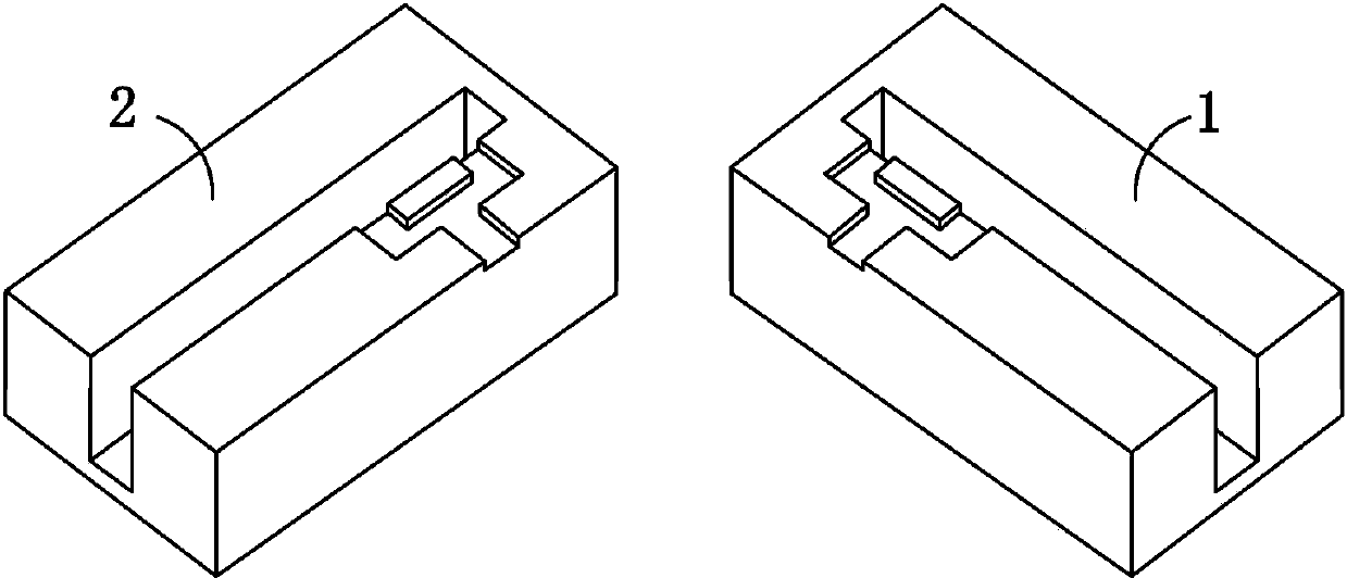
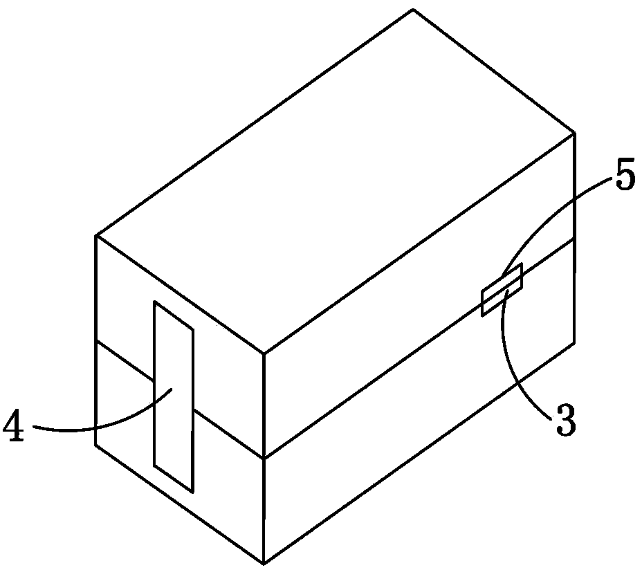
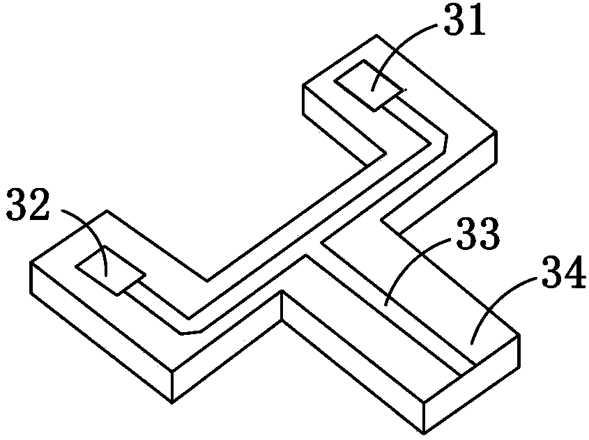
[0026] Such as figure 1 , figure 2 As shown, the microstrip waveguide double-probe transition structure in this embodiment includes an upper cavity 1, a lower cavity 2, and a microstrip circuit 3, and the upper cavity 1 covers the lower cavity 2 to form a rectangular waveguide cavity 4 and Microstrip circuit shielding cavity 5, the microstrip circuit 3 is fixed in the microstrip circuit shielding cavity 5, such as image 3 As shown, the microstrip circuit 3 includes two microstrip probes 31, 32, a power distribution / synthesis circuit 33 and a dielectric substrate 34, and the two microstrip probe...


PUM


Abstract

The invention discloses a microstrip waveguide double-probe transition structure applicable to a millimeter-wave frequency multiplier. The structure includes an upper cavity, a lower cavity and a microstrip circuit. The lower cavity is covered with the upper cavity in a sealing way so that a rectangular waveguide cavity and a microstrip circuit shielding cavity are formed. The microstrip circuit is fixed in the microstrip-circuit shielding cavity. The microstrip circuit includes two microstrip probes, a power distribution/synthesis circuit and a dielectric substrate. The two microstrip probes and the power distribution / synthesis circuit are arranged on the same surface of the dielectric substrate. The two microstrip probes are connected with the two ends of the power distribution / synthesis circuit respectively. A distance between the center line of one microstrip probe and a rectangular-waveguide short-circuit face is 1/4 of a waveguide wavelength of an objective frequency and a distance between the center line of the other microstrip probe and the rectangular-waveguide short-circuit face is 5/4 of the waveguide wavelength of the objective frequency. The microstrip waveguide double-probe transition structure is capable of realizing same-phase superposition of an objective frequency signal and reversed-phase offset and output inhibition of a non-objective-frequency signal. The transition structure is simple in structure, convenient to manufacture and low in price.

Description

technical field [0001] The invention belongs to the technical field of millimeter wave devices, and in particular relates to a microstrip waveguide double-probe transition structure suitable for a millimeter wave frequency multiplier. Background technique [0002] Millimeter wave is a broad frequency range from 30GHz to 300GHz. Compared with light waves, millimeter waves have less attenuation when propagating through the atmospheric window (when millimeter waves and submillimeter waves propagate in the atmosphere, some attenuation is minimal due to the resonance absorption of gas molecules), and are affected by natural light and heat radiation. The source influence is small; compared with radio frequency and microwave, it has an extremely wide bandwidth, which is very attractive in today's tight frequency resources; it also has the advantages of narrow beam, less affected by climate and corresponding small device size. [0003] The transition structure is to realize the tra...

Claims


Application Information

Patent Timeline
Patent Type & Authority Applications(China)
IPC IPC(8): H01P3/08
Inventor 张勇钟伟王云飞詹铭周胡天涛徐跃杭
Owner UNIV OF ELECTRONICS SCI & TECH OF CHINA
Why Eureka
Try Eureka