Method for defect detection and surface measurement of silicon wafer

A defect detection, silicon wafer technology, applied in measuring devices, optical testing flaws/defects, using optical devices, etc., can solve problems such as damage to the surface of the object to be measured, complex design, and inability to measure free-form objects

Active Publication Date: 2014-01-01
UNIV OF ELECTRONICS SCI & TECH OF CHINA
View PDF5 Cites 43 Cited by
  • Summary
  • Abstract
  • Description
  • Claims
  • Application Information

AI Technical Summary

Problems solved by technology

However, these measurement systems have high requirements for measurement conditions, slow measurement speed or low measurement accuracy, and are not suitable for high-precision three-dimensional surface shape detection of semiconductor wafers. For example, the measurement time of the contact three-coordinate machine is quite long (usually several Hours or

Method used


Image

  • Method for defect detection and surface measurement of silicon wafer
  • Method for defect detection and surface measurement of silicon wafer
  • Method for defect detection and surface measurement of silicon wafer

Examples


Embodiment Construction

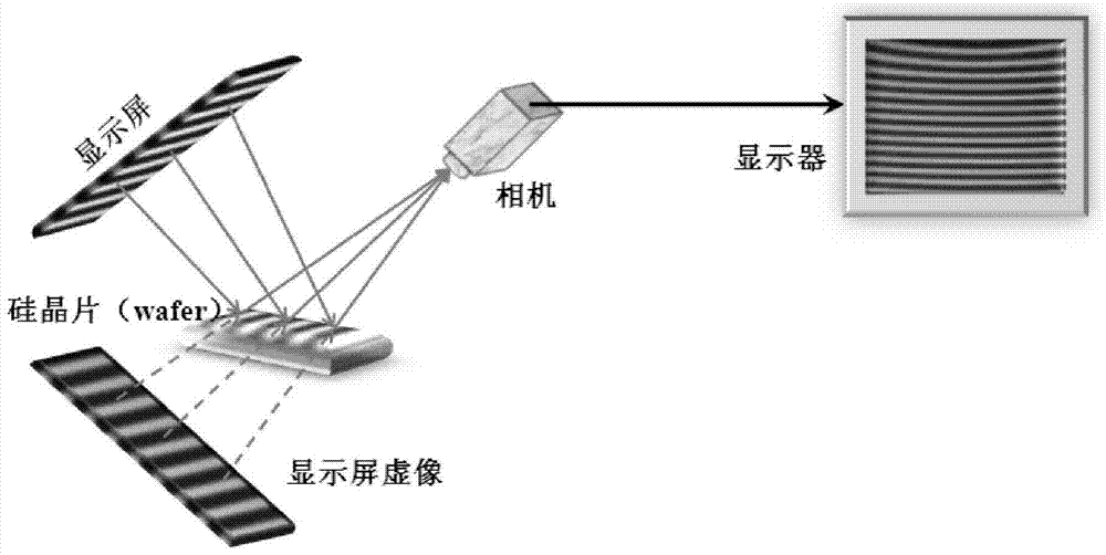
[0031] The invention discloses a method for silicon wafer defect detection and surface shape measurement. The method uses phase deflection profilometry (PMD) in the silicon wafer surface shape measurement. Embodiments of the invention will be described in detail below in conjunction with the accompanying drawings and specific implementation examples.

[0032] Step 1: Set up the experimental measurement system: the system mainly includes a camera, a display screen, an object to be measured, a control computer and a stand. The system is adjusted so that the camera sees the fringes on the display through the silicon wafer of the object under test. Such as figure 1 .

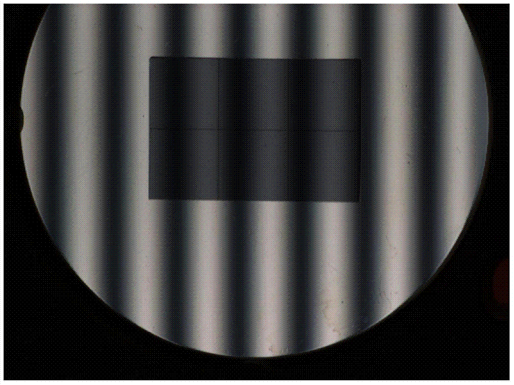
[0033] Step 2: The display screen is controlled by a computer to produce standard horizontal and vertical sinusoidal stripes, and the camera captures the deformed stripes reflected by the wafer. In this example, the CCD camera is Manta G-125B / C, and the camera uses a 50mm fixed-focus lens (Computar M5018-MP2).

...


PUM


Abstract

The invention provides a method for defect detection and surface measurement of a silicon wafer. According to the method, the phase-measuring deflectometry(PMD) is used for surface measurement of a silicon wafer. The PMD-based mirror object three-dimensional surface measurement method is a highly-sensitive, high-precision, quick and incoherent optical full-field measurement technology, and an experimental device is simple and mainly comprises a computer, a digital camera and a display screen. When the PMD is used for surface measurement of the silicon wafer, the surface gradient distribution of the silicon wafer can be directly obtained, the surface curvature distribution of the silicon wafer can be obtained so long as gradient derivation is performed, defects are detected through curvature distribution, the surface height data of the silicon wafer can be obtained through gradient integration, and accordingly, the three-dimensional shape can be observed. The invention has the main gain that the high-precision and quick full-field measurement technology is provided to realize surface defect detection and surface measurement of the silicon wafer.

Description

technical field [0001] The invention relates to the technical field of using a three-dimensional measurement method based on phase deflection profilometry for defect detection and surface shape measurement of silicon wafers. Background technique [0002] With the development of precision optical processing, automotive painting, industrial manufacturing and product quality inspection, people are increasingly eager to accurately measure mirrors or mirror-like reflection objects, such as the detection of free-form mirrors or lenses (such as glasses), The control of spray paint quality (orange peel phenomenon) on the surface of automobiles, the quality evaluation of surface processing of precision devices, etc. Through the measurement and analysis of various mirror or mirror-like surfaces, the influence of various parameters (such as grinding speed, grinding materials, mechanical vibration, etc.) in the corresponding manufacturing process on the surface processing quality can be...

Claims


Application Information

Patent Timeline
IPC IPC(8): G01N21/88G01B11/24
Inventor 岳慧敏吴雨祥刘永赵必玉张博易京亚欧中华
Owner UNIV OF ELECTRONICS SCI & TECH OF CHINA
Why Eureka
Try Eureka