Sheet bonding method in substrate thinning technique

A substrate and process technology, which is applied in the field of microwave power field effect transistor and integrated circuit technology, to achieve the effects of avoiding mutual dissolution, increasing process complexity, improving process efficiency and process yield

Inactive Publication Date: 2014-01-01
INST OF MICROELECTRONICS CHINESE ACAD OF SCI
View PDF3 Cites 15 Cited by
  • Summary
  • Abstract
  • Description
  • Claims
  • Application Information

AI Technical Summary

Problems solved by technology

[0011] In view of this, the main purpose of the present invention is to provide a method for bonding chips in the substrate thinning process to effectively solve the problem of mutual solubility of photoresist and high-temperature wax, and improve the process efficiency and process yield of the thinning process

Method used


Image

  • Sheet bonding method in substrate thinning technique
  • Sheet bonding method in substrate thinning technique
  • Sheet bonding method in substrate thinning technique

Examples


Embodiment Construction

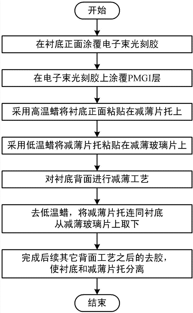
[0028] In order to make the object, technical solution and advantages of the present invention clearer, the present invention will be described in further detail below in conjunction with specific embodiments and with reference to the accompanying drawings.

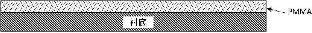
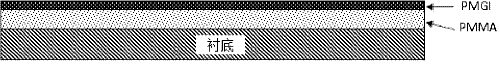
[0029] The chip bonding method in the substrate thinning process provided by the present invention is to use the PMMA950-A11 / PMGI / high temperature wax structure, insert the PMGI layer between the PMMA950-A11 electron beam photoresist and the high temperature wax, and utilize the intrinsic properties of PMGI Properties, prevent the miscibility of two organic compounds from occurring. In this way, after the thinning process and other backside processes are completed, the substrate and the wafer holder can be successfully separated by the degumming process, which greatly shortens the process time and avoids the generation of insoluble organic matter.

[0030] Such as figure 1 as shown, figure 1 It is a flow chart of the ch...


PUM

PropertyMeasurementUnit
thicknessaaaaaaaaaa
thicknessaaaaaaaaaa

Abstract

The invention discloses a sheet bonding method in a substrate thinning technique, which comprises the following steps: coating an electron beam photoresist on the front surface of a substrate; coating a PMGI layer on the electron beam photoresist; bonding the front surface of the substrate onto a thinning sheet support by using high temperature wax; bonding the thinning sheet support onto a thinning glass sheet by using low temperature wax; carrying out thinning technique on the back surface of the substrate; removing the low temperature wax, and taking the thinning sheet support with the substrate off the thinning glass sheet; and completing subsequent photoresist removal after other back surface techniques, and separating the substrate from the thinning sheet support. The method effectively solves the problem of mutual solubility between the photoresist and high temperature wax, and enhances the technical efficiency and technical yield of the thinning technique.

Description

technical field [0001] The invention relates to a chip bonding method in a substrate thinning process, especially for microwave power field-effect transistor (FET) and integrated circuit technology, which can effectively avoid the fusion between high-temperature wax and photoresist, and is extremely Greatly improve the efficiency and quality of glue removal, and finally achieve the purpose of improving the yield of devices and circuits. Background technique [0002] With the development of microwave power devices and circuits, devices and circuits have higher and higher requirements on the efficiency and yield of subsequent processes. In the thinning step in the subsequent process, the die bonding process is essential, and the die bonding and the separation process of the substrate and the chip support after thinning directly affect the yield of devices and circuits. [0003] In order to facilitate the heat dissipation of devices and circuits and reduce high-frequency paras...

Claims


Application Information

Patent Timeline
Patent Type & Authority Applications(China)
IPC IPC(8): H01L21/02
CPCH01L21/6835H01L2221/68381
Inventor 郑英奎杜萌王鑫华
Owner INST OF MICROELECTRONICS CHINESE ACAD OF SCI
Why Eureka
Try Eureka