
A two-step evanescent field coupled avalanche photodetector

An avalanche optoelectronic and evanescent field technology, which is applied to circuits, electrical components, semiconductor devices, etc., can solve problems such as low sensitivity, unfavorable on-chip optical interconnection, mutual constraints between responsivity and bandwidth, and achieve reduced coupling loss and high sensitivity. The effect of light detection

Active Publication Date: 2015-12-23
INST OF SEMICONDUCTORS - CHINESE ACAD OF SCI
View PDF6 Cites 0 Cited by
  • Summary
  • Abstract
  • Description
  • Claims
  • Application Information

AI Technical Summary

Problems solved by technology

[0005] The main purpose of the present invention is to provide a waveguide avalanche detector with high responsivity and high bandwidth dual-step evanescent field coupling to solve the problem of large optical loss, low sensitivity, mutual constraints between responsivity and bandwidth, and unfavorable on-chip optical Interconnection and other issues

Method used


Image

  • A two-step evanescent field coupled avalanche photodetector
  • A two-step evanescent field coupled avalanche photodetector
  • A two-step evanescent field coupled avalanche photodetector

Examples


Embodiment Construction

[0027] In order to make the object, technical solution and advantages of the present invention clearer, the present invention will be described in further detail below in conjunction with specific embodiments and with reference to the accompanying drawings.

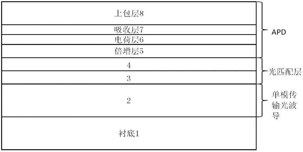
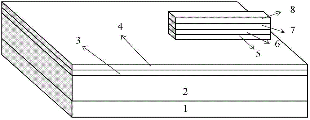
[0028] Such as Figure 5 Shown is a schematic diagram of the structure of the double-step evanescent field coupled avalanche photodetector proposed by the present invention. The double-step evanescent field coupled avalanche photodetector includes: a substrate 1; a single-mode transmission light formed on the substrate 1 a waveguide 2; an optical matching layer formed on the single-mode transmission optical waveguide 2; and an avalanche photodetector (APD) mesa formed on the optical matching layer. The protruding length of the single-mode transmission optical waveguide 2 relative to the optical matching layer is determined by the cleavage process, preferably 50 μm; the protruding length of the optical matching layer relat...


PUM

PropertyMeasurementUnit
Thicknessaaaaaaaaaa
Thicknessaaaaaaaaaa
Lengthaaaaaaaaaa

Abstract

The invention discloses an APD with the dual-step evanescent field coupling function. The APD comprises a substrate, a single-mode transmission light waveguide, a light matching layer and an APD table top. The single-mode transmission light waveguide is formed on the substrate and used for achieving low-loss single-mode transmission of matched light spots in the waveguide and allowing light to be gradually evanescent field coupled upwards to enter the light matching layer. The light matching layer is formed on the single-mode transmission light waveguide and used for allowing the light power to be efficiently evanescent field coupled to an APD absorbing layer from the single-mode transmission light waveguide and limiting light in the APD absorbing layer to be completely absorbed. The APD table top is formed on the light matching layer, and a separate absorbing charge multiplication area structure and a waveguide structure are integrated to achieve optical detection which is high in speed and responsivity. The APD with the internal gain and high sensitivity and the single-mode waveguide structure with the evanescent field coupling function are integrated, and the problems that a common detector is large in loss and low in sensitivity, responsivity and bandwidths are mutually restricted, and then on-chip optical interconnection is not facilitated are solved.

Description

technical field [0001] The invention relates to the technical field of edge incident light high-performance waveguide detector design, in particular to an avalanche photodetector coupled by two-step evanescent fields. Background technique [0002] Photodetectors are important components in photonics systems, and the performance of detectors is an important factor restricting the performance of photonics systems. In the future, as photonic systems have higher and higher requirements for high bandwidth and high integration, the traditional detector structure has been difficult to meet the needs of high-bandwidth and high-responsive photonic systems: In order to ensure the necessary photosensitive surface , the electrical size is difficult to reduce, and the bandwidth of the device is limited; to meet the needs of high bandwidth performance, the optical response performance must be sacrificed; and the integration of surface incident devices and waveguide functional structures i...

Claims


Application Information

Patent Timeline
IPC IPC(8): H01L31/107H01L31/0232
CPCH01L31/02327H01L31/1075
Inventor 崔荣杨晓红李彬尹伟红吕倩倩韩勤
Owner INST OF SEMICONDUCTORS - CHINESE ACAD OF SCI
Learn More