Antistatic structure of array substrate

An array substrate, anti-static technology, applied in the direction of circuits, electrical components, electric solid devices, etc., can solve problems affecting product quality, electrostatic damage, etc., to achieve the effects of avoiding electrostatic damage, improving product quality, and reducing production costs

Active Publication Date: 2014-01-08
TCL CHINA STAR OPTOELECTRONICS TECH CO LTD
View PDF5 Cites 14 Cited by
  • Summary
  • Abstract
  • Description
  • Claims
  • Application Information

AI Technical Summary

Problems solved by technology

[0009] Abnormal discharge will still cause electrostatic damage to the 100 overlapping metal wires of the shorting bar, affecting product quality

Method used


Image

  • Antistatic structure of array substrate
  • Antistatic structure of array substrate
  • Antistatic structure of array substrate

Examples


Embodiment Construction

[0031] In order to further illustrate the technical means adopted by the present invention and its effects, the following describes in detail in conjunction with preferred embodiments of the present invention and accompanying drawings.

[0032] The present invention is described in the VA display mode, but is not limited to the VA display mode.

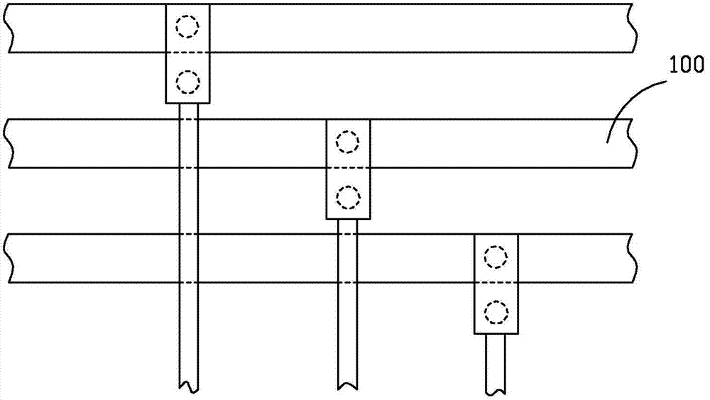
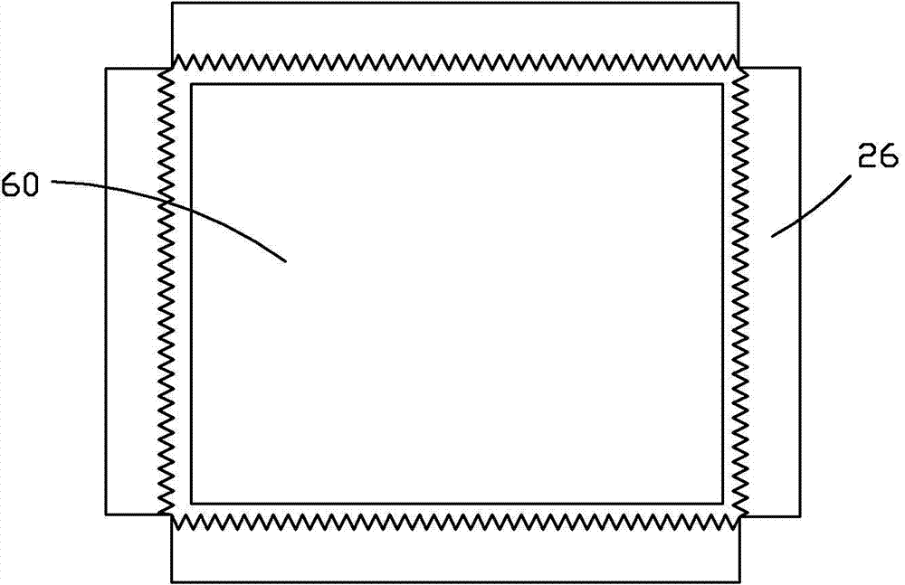
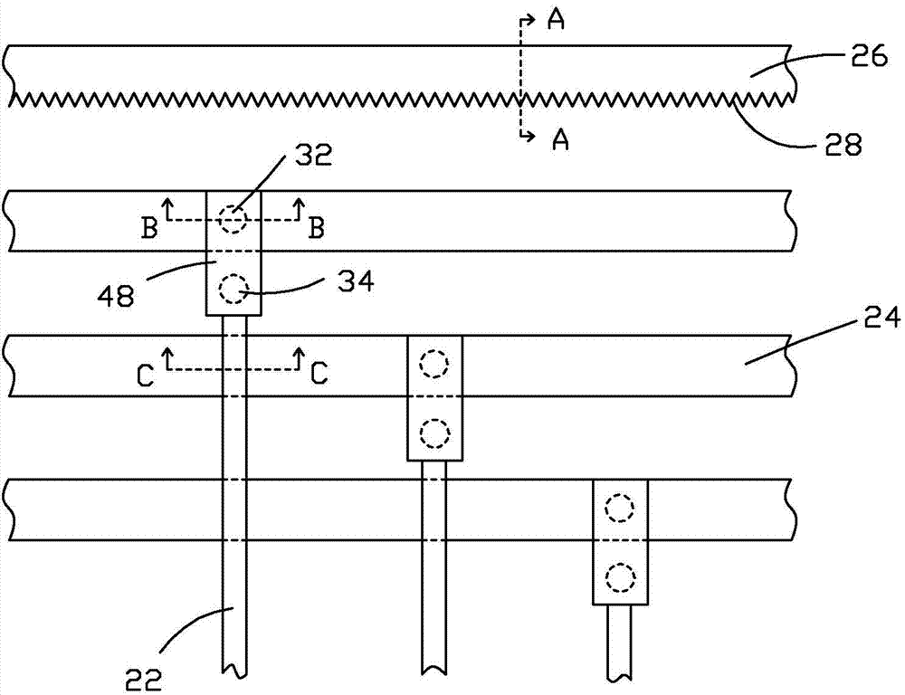
[0033] The present invention is to pattern imaginary lines parallel to the short-circuit bar next to the short-circuit bar during the fabrication of the array substrate, that is, the present invention provides an anti-static structure for the array substrate. Please refer to figure 2 and image 3 , specifically including: an active area 60 of the array substrate and several imaginary lines 26 surrounding the effective area 60, the active area 60 of the array substrate is provided with several signal lines 22 and electrically connected to the several signal lines 22 respectively. Several shorting bars 24, the imaginary lines 26 are a...


PUM


Abstract

The invention provides an antistatic structure of an array substrate. The antistatic structure comprises an effective zone (60) of the array substrate and a plurality of imaginary lines (26) surrounding the effective zone (60); the effective zone is provided with a plurality of signal lines (22) and a plurality of short circuit bars (24) electrically connected with the signal lines (22); the imaginary lines (26) are adjacently arranged by respectively corresponding to the short bars (24) positioned at the outermost periphery of the effective zone (60); one sides (28), close to the short circuit bars (24), of the imaginary lines (26) are arranged in a saw tooth-shaped structure. One imaginary line is additionally added beside each short circuit bar at the outermost periphery, and one sides, close to the short circuit bars, of the imaginary lines are arranged in a saw tooth-shape structure, in such a mode, in the manufacturing process of the array substrate and particularly during the dry etching for an insulation protective layer and an active layer, the static damage to the metal overlapping wires at the short circuit bars caused by abnormal discharging of a plasma can be better avoided, and the product quality can be improved.

Description

technical field [0001] The present invention relates to the field of display technology, in particular to an antistatic structure of an array substrate. Background technique [0002] A liquid crystal display (Liquid Crystal Display, LCD) has many advantages such as a thin body, power saving, and no radiation, and has been widely used. Most of the liquid crystal display devices currently on the market are backlight liquid crystal display devices, which include a housing, a liquid crystal display panel disposed in the housing, and a backlight module disposed in the housing and opposite to the liquid crystal display panel. The working principle of the liquid crystal display panel is to place liquid crystal molecules between two parallel glass substrates, and apply a driving voltage on the two glass substrates to control the rotation of the liquid crystal molecules, thereby refracting the light from the backlight module to produce a picture. [0003] Electro-Static discharge (E...

Claims


Application Information

Patent Timeline
Patent Type & Authority Applications(China)
IPC IPC(8): H01L23/60
CPCG02F1/136204H01L27/124H01L27/0288G02F1/1368
Inventor 徐向阳张伟闵宋志扬王亮
Owner TCL CHINA STAR OPTOELECTRONICS TECH CO LTD
Why Eureka
Try Eureka