Broadband long-wave-response GaAs/AlxGa1-xAs quantum well infrared detector and manufacturing method and application thereof

A technology of infrared detectors and quantum wells, used in semiconductor devices, final product manufacturing, sustainable manufacturing/processing, etc., can solve the loss of optical signal, cannot meet the requirements of detector uniformity and large-area array, and affect thermal imaging quality and other issues

Inactive Publication Date: 2014-01-08
SHANDONG UNIV
View PDF3 Cites 6 Cited by
  • Summary
  • Abstract
  • Description
  • Claims
  • Application Information

AI Technical Summary

Problems solved by technology

The silicon-based compound detectors in the 1960s had a cut-off response wavelength that was difficult to reach the long-wavelength band. After 1980, HgCdTe detectors became more and more mature, but they were increasingly unable to meet people’s needs for detector uniformity and large-area arrays. QWIP detector is a high-tech in the world in recent years
QWIP detector has the advantages of fast response speed, detection rate similar to that of HgCdTe detector, and manual modulation of detection wavelength, etc., but its spectral response bandwidth is narrower than that of HgCdTe detector.
[0003] The narrow spectral response bandwidth brings the loss of optical signals of some wavelengths, which affects the quality of thermal imaging. S.V.Bandara et al reported that several quantum wells with different well widths and well depths are used to form a basic unit for the GaAs / AlGaAs material system. Then a quantum well infrared detector is made with multiple such basic units, and its spectral bandwidth has reached Δλ / λ P =42%, but its production process is quite complicated

Method used


Image

  • Broadband long-wave-response GaAs/AlxGa1-xAs quantum well infrared detector and manufacturing method and application thereof

Examples


Embodiment Construction

[0007] Technical scheme of the present invention is as follows:

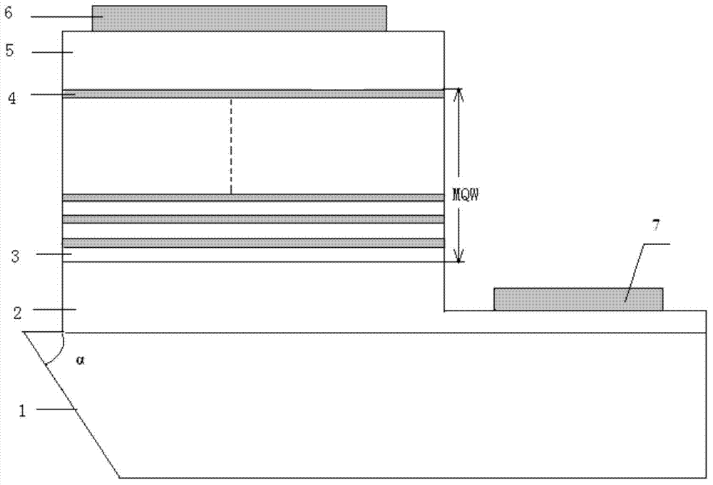
[0008] A Broadband and Longwave Response GaAs / Al x Ga 1-x The As quantum well infrared detector includes a GaAs substrate and a GaAs bottom contact layer arranged sequentially from bottom to top, and the GaAs bottom contact layer includes a raised mesa structure, and multiple layers are sequentially arranged on the mesa structure. The quantum well layer MQW, the GaAs top contact layer and the upper electrode are also provided with a lower electrode on the GaAs bottom contact layer; the multiple quantum well layer MQW is Al x Ga 1-x As layer and GaAs layer; according to the infrared photon frequency and spectral broadening required for detection, the quantum interference model is used to design the barrier width, potential well width, composition, and doping concentration of the quantum well region:

[0009] The alternate growth period of the quantum well layer MQW is 40-60, and the preferred selection period ...


PUM


Abstract

The invention provides a broadband long-wave-response GaAs / AlxGa1-xAs quantum well infrared detector, which comprises a GaAs substrate and a GaAs bottom contact layer arranged in sequence from bottom to top, wherein the GaAs bottom contact layer comprises a projecting table-shaped structure; a multi-quantum-well (MQW) layer, a GaAs top contact layer and an upper electrode are arranged in sequence on the table-shaped structure; the GaAs bottom contact layer is further provided with a lower electrode; the MQW layer consists of an AlxGa1-xAs layer and a GaAs layer growing periodically and alternately; the infrared detector is used for introducing a plurality of discrete micro-strips above the top of a barrier via fine design of the parameters of a super lattice structure according to an electron interference theory in a super lattice quantum well structure; photoelectrons jump under the action of an external electric field to form a plurality of corresponding photocurrent peaks which are overlapped together, so that the spectral bandwidth is increased.

Description

technical field [0001] The invention relates to GaAs / Al with broadband and long-wave response x Ga 1-x An As quantum well infrared detector and its preparation method and application belong to the technical field of semiconductor infrared detectors. Background technique [0002] As an important development direction in today's high-tech field, infrared detectors have made remarkable achievements in many fields such as civil, military, and space. The silicon-based compound detectors in the 1960s had a cut-off response wavelength that was difficult to reach the long-wavelength band. After 1980, HgCdTe detectors became more and more mature, but they were increasingly unable to meet people’s needs for detector uniformity and large-area arrays. QWIP detector is a high-tech in the world in recent years. QWIP detector has the advantages of fast response speed, detection rate similar to that of HgCdTe detector, and manual modulation of detection wavelength, etc., but its spectral...

Claims


Application Information

Patent Timeline
Patent Type & Authority Applications(China)
IPC IPC(8): H01L31/0352H01L31/0304H01L31/18
CPCH01L31/03044H01L31/03048H01L31/035263H01L31/101H01L31/1848H01L31/1856Y02P70/50
Inventor 连洁赵明琳张福军孙兆宗王晓高尚张文赋胡娟娟夏伟
Owner SHANDONG UNIV
Why Eureka
Try Eureka