
Optical proximity effect correction method

A technology of optical proximity effect and lithography process, applied in optics, original parts for opto-mechanical processing, instruments, etc., can solve the problem of lithography line width drift, etc., to avoid waste and avoid lithography line width drift. Effect

Active Publication Date: 2014-01-15
SHANGHAI HUAHONG GRACE SEMICON MFG CORP
View PDF6 Cites 6 Cited by
  • Summary
  • Abstract
  • Description
  • Claims
  • Application Information

AI Technical Summary

Problems solved by technology

[0006] The technical problem to be solved by the present invention is to provide an optical proximity effect correction method, which can solve the problem of photolithographic line width drift caused by large-area topography or substrate changes

Method used


Image

  • Optical proximity effect correction method
  • Optical proximity effect correction method
  • Optical proximity effect correction method

Examples


Embodiment Construction

[0018] In order to have a more specific understanding of the technical content, characteristics and effects of the present invention, now in conjunction with the illustrated embodiment, the details are as follows:

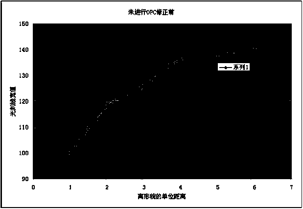
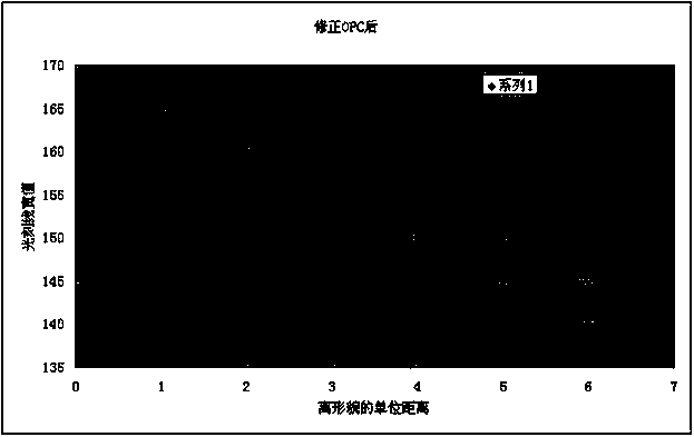
[0019] The flow process of OPC correction method of the present invention is as follows:

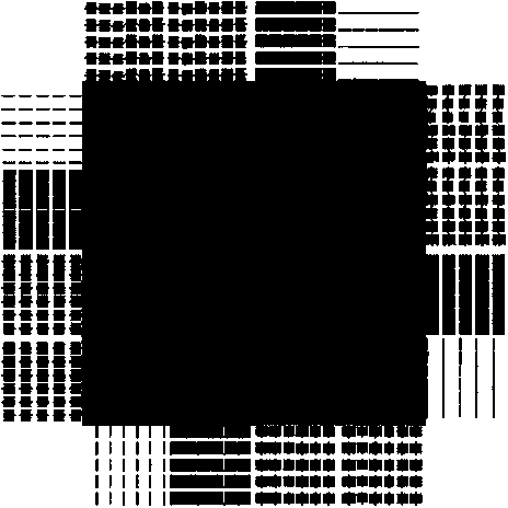
[0020] Step 1. Make two test photoresist plates, wherein, the first photoresist plate is designed according to the topography of the front layer, and is used to place the front layer graphics, that is, the graphics of the front layer that produces morphology or film layer changes; the second photolithography plate The engraving plate is used to place the test pattern of the rear OPC around the topographical pattern according to certain rules.

[0021] The method of placing the OPC test pattern is: repeat the placement according to the distance from the pattern that generates the shape. Place the OPC test pattern in the Y direction (that is, the direction perpendicular to the...


PUM


Abstract

The invention discloses an optical proximity effect correction method comprising the following processes: 1) two test photolithography plates are made, a front-layer morphology pattern is placed on a first test photolithography plate, and a back-layer OPC (optical proximity correction) test pattern is placed on a second test photolithography plate; 2) the second test photolithography plat is gelatinized for exposure and development, and photolithography process key size values are collected for establishing an OPC model; 3) the first test photolithography plat is gelatinized for exposure and development to generate a front-layer pattern morphology; 4) the second test photolithography plat is gelatinized for exposure and development, and the photolithography process key size values are collected for establishing a selected bias algorithm (SSA) for characterization of different regional deviation values to be increased; and 5) in a region with the morphology, optical proximity correction (OPC) is redone according to the deviation values. According to the method, first the normal OPC model is established, when large-area morphology or substrate is changed, OPC test pattern data is again collected, a SSA form is established, and the optical proximity correction (OPC) is redone in the region with the morphology, so that photolithography line width drift and chip area waste caused by large-area morphology or substrate change can be avoided.

Description

technical field [0001] The invention relates to the field of semiconductor integrated circuit manufacturing, in particular to a method for correcting the optical proximity effect. Background technique [0002] In the semiconductor lithography process, in order to improve the resolution limit, the technology node of 0.13 microns starts to use the Optical Proximity Correction (OPC, Optical Proximity Correction) technology. Among them, the model-based OPC correction method is the main OPC correction method currently used. This method is to expose on the actual lithographic substrate with the best lithographic conditions, and then collect various test patterns (including one-dimensional and Two-dimensional graphics) lithography key dimension value, through these measured values ​​to establish a model of lithography process, to simulate the whole process of lithography, including exposure and development process. Then, according to the model calculation, the line width size of t...

Claims


Application Information

Patent Timeline
IPC IPC(8): G03F1/36
Inventor 陈福成
Owner SHANGHAI HUAHONG GRACE SEMICON MFG CORP
Learn More