Chip structure and manufacturing method thereof

A technology of chip structure and manufacturing method, which is applied in semiconductor/solid-state device manufacturing, semiconductor devices, electrical components, etc., and can solve problems such as waste of chip area, limited chip withstand voltage capability, and large chip terminal width

Active Publication Date: 2016-11-23
BYD SEMICON CO LTD
View PDF5 Cites 0 Cited by
  • Summary
  • Abstract
  • Description
  • Claims
  • Application Information

AI Technical Summary

Problems solved by technology

[0004] The purpose of the present invention is to at least solve one of the above-mentioned technical defects, especially the defects of the existing field-limiting ring structure that the chip terminal width is too large, the terminal utilization rate is not high, the chip area is wasted, and the chip withstand voltage is limited.

Method used


Image

  • Chip structure and manufacturing method thereof
  • Chip structure and manufacturing method thereof
  • Chip structure and manufacturing method thereof

Examples


Embodiment Construction

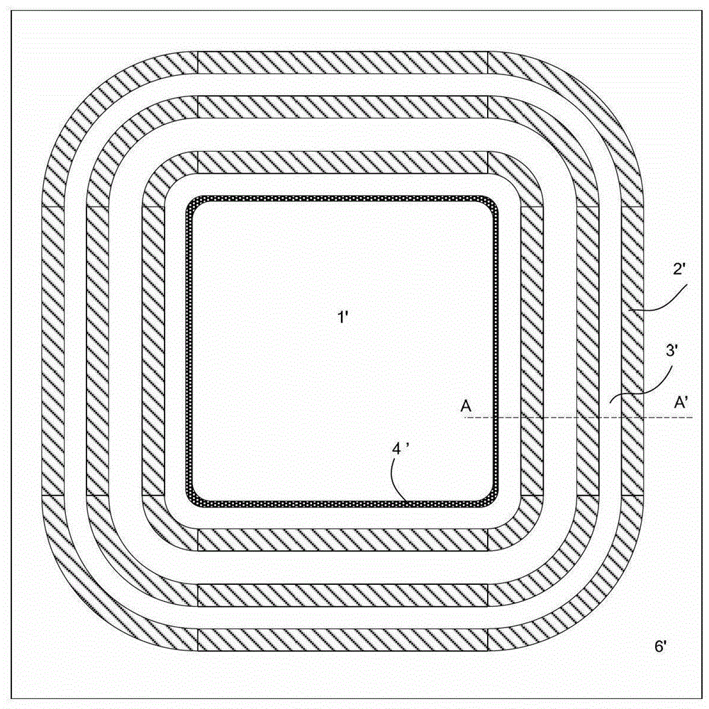
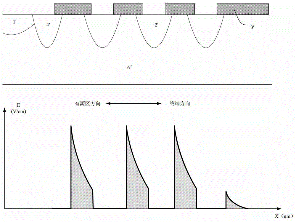
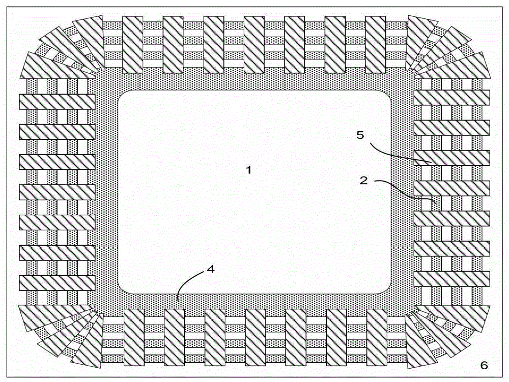
[0033] Embodiments of the present invention are described in detail below, examples of which are shown in the drawings, wherein the same or similar reference numerals designate the same or similar elements or elements having the same or similar functions throughout. The embodiments described below by referring to the figures are exemplary only for explaining the present invention and should not be construed as limiting the present invention.

[0034]In describing the present invention, it should be understood that the terms "center", "longitudinal", "transverse", "upper", "lower", "front", "rear", "left", "right", " The orientations or positional relationships indicated by "vertical", "horizontal", "top", "bottom", "inner", "outer", etc. are based on the orientation or positional relationships shown in the drawings, and are only for the convenience of describing the present invention and simplifying Describes, but does not indicate or imply that the device or element referred ...


PUM


Abstract

The invention provides a chip structure and a manufacturing method thereof. The chip structure comprises a substrate, an active region formed at the active region in the substrate, and a terminal region formed in the substrate, wherein the active region includes a logic circuit of the chip. Besides, the terminal region includes a main node encircling the active region, a plurality of filed limiting rings successively and concentrically encircling the main node, and a plurality of grooves; insulated layers are formed at the inner walls of the grooves; conductive layers are formed on the insulated layers in the grooves; and preset angles are formed between the grooves and the field limiting rings. Because the grooves with the conductive layers are arranged in the terminal region, an objective of improvement of the voltage-withstanding capability of the chip terminal can be achieved. According to the chip structure provided by the embodiment of the invention, the terminal width can be effectively reduced, the chip area and the chip cost are reduced; and the stability of the device can be substantially enhanced.

Description

technical field [0001] The invention relates to the field of semiconductor design and manufacture, in particular to a chip structure and a manufacturing method thereof. Background technique [0002] With the development of semiconductor technology, semiconductor power devices tend to develop towards high current and high voltage. However, as the operating voltage of the device increases, the withstand voltage requirements for the chip terminals are also getting higher and higher. In the prior art, the chip size is required to be large enough. Because after the reverse bias voltage is applied to the chip, the doped region in the active region will gradually broaden the electric field, and the potential difference will be added to the depletion region, thereby protecting the chip. The broadened electric field approximates a planar junction, so that the active region can easily reach a higher breakdown voltage. However, since the scribing lane and the back of the chip are at ...

Claims


Application Information

Patent Timeline
Patent Type & Authority Patents(China)
IPC IPC(8): H01L29/06H01L29/78H01L21/336
CPCH01L29/401H01L29/407H01L29/66348H01L29/7397
Inventor 刘鹏飞吴海平
Owner BYD SEMICON CO LTD
Why Eureka
Try Eureka