Bipolar punch-through semiconductor device and method for manufacturing such a semiconductor device

A semiconductor and device technology, applied in the field of bipolar punch-through semiconductor devices, can solve the problems of wafer diameter limitation and many difficulties in thin wafers

Active Publication Date: 2014-01-15
HITACHI ENERGY SWITZERLAND AG
View PDF11 Cites 2 Cited by
  • Summary
  • Abstract
  • Description
  • Claims
  • Application Information

AI Technical Summary

Problems solved by technology

In addition, the larger the wafer diameter, the more difficulties encountered in thin wafer processing
Therefore, prior art methods are limited by smaller wafer diameters
Finally, the quality and availability of silicon substrate material is also an issue for thin wafer technologies using e.g. deep diffusion methods (especially for larger wafer diameters above 200mm)

Method used


Image

  • Bipolar punch-through semiconductor device and method for manufacturing such a semiconductor device
  • Bipolar punch-through semiconductor device and method for manufacturing such a semiconductor device
  • Bipolar punch-through semiconductor device and method for manufacturing such a semiconductor device

Examples


Embodiment Construction

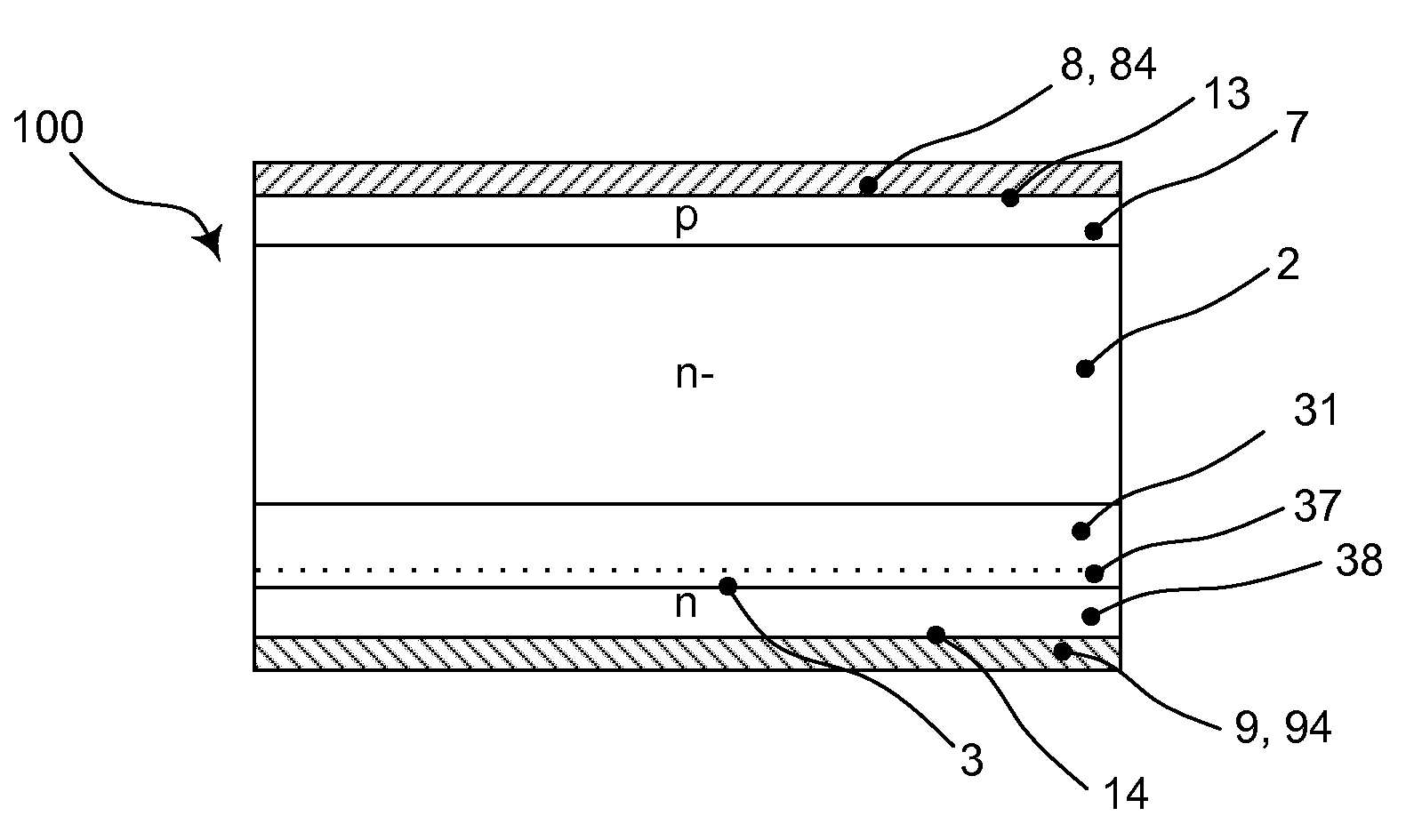
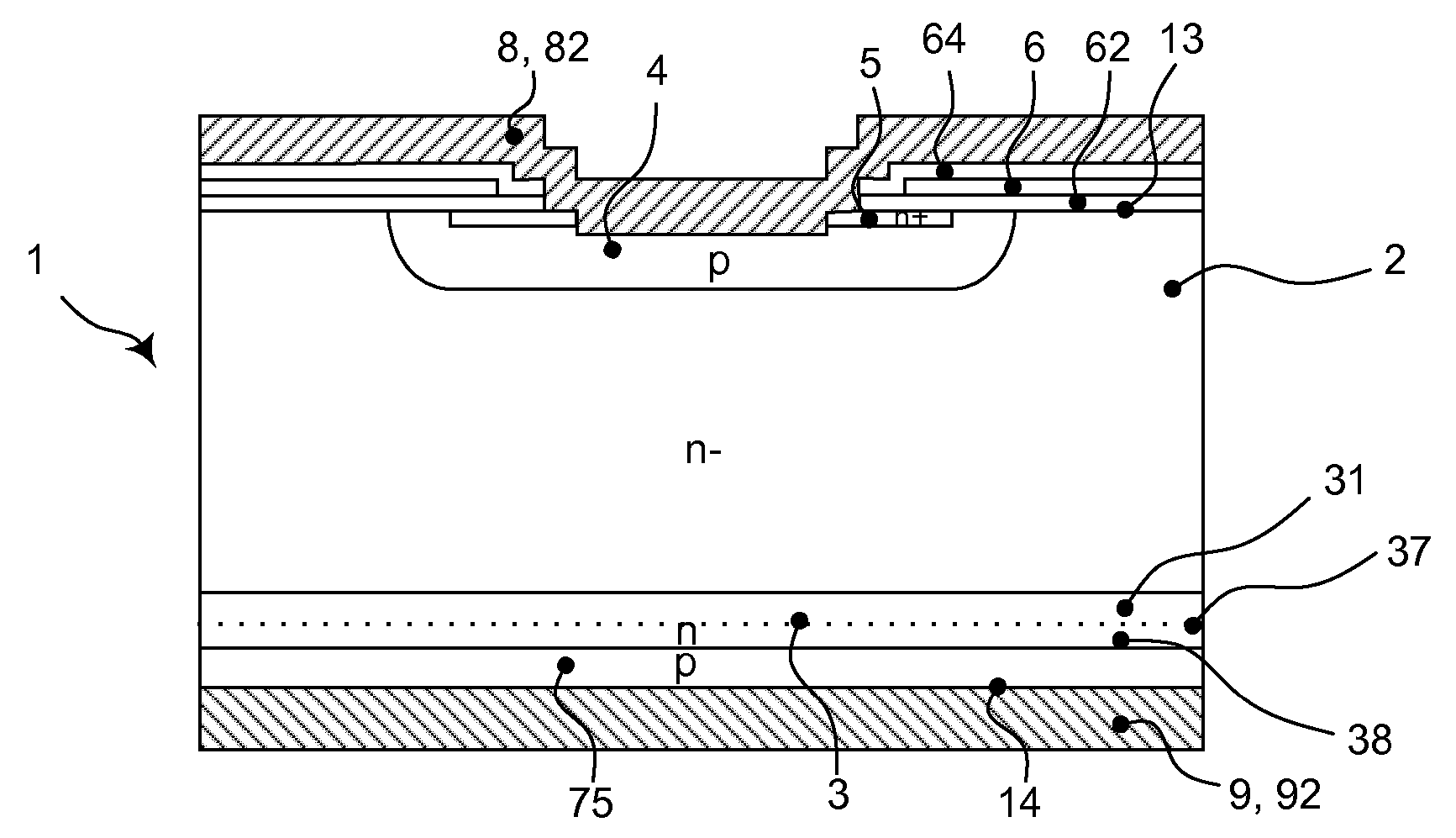
[0034] The bipolar punchthrough semiconductor device according to the invention as shown in FIGS. 3 , 11 to 12 comprises a first main side 13 and a second main side 14 which are arranged on opposite sides of the first main side 13 . The first electrical contact 8 is arranged on the first main side 13 and the second electrical contact 9 is arranged on the second main side 14 . The device has at least a bilayer structure having layers of a first and a second conductivity type, the second conductivity type being different from the first conductivity type. One of these layers is a low doped drift layer 2 of the first conductivity type, ie n-type in the figure.

[0035] as in Figure 3a ) to c) is an Insulated Gate Bipolar Transistor (IGBT) 1 in which the first electrical contact 8 is formed as an emitter electrode 82 and the second electrical contact 9 is formed as a collector electrode 92 .

[0036] A p-type layer in the form of base layer 4 is arranged on first main side 13 (e...


PUM


Abstract

A method for manufacturing a bipolar punch-through semiconductor device is provided, wherein the following steps are performed (a)providing a first high-doped wafer (10) having a first and a second side (11, 2), which is doped at least on the first side (11) with first particles of the first conductivity type, (b)providing a second low-doped wafer (20) of the first conductivity type having a third and a fourth side, (c)creating a wafer laminate having a wafer laminate thickness by bonding the first wafer (10) on its first side (11) and the second wafer (20) on its fourth side (22) together, (d)performing afterwards a diffusion step,thereby creating a diffused inter- space layer (31), which comprises first sided parts of the first wafer (10) and fourth sided parts of the second wafer (20), wherein that part of the second wafer having unamended doping concentration in the finalized device forms a drift layer (2), (e)afterwards creating at least one layer of the second conductivity type on the third side (21), (f)afterwards reducing the wafer laminate thickness from the second side (12) within the inter-space layer (31) and within the second wafer (20) such that a buffer layer(3) is created, which comprises the remaining part of the wafer laminate on the fourth side (22) having higher doping concentration than the drift layer (2).

Description

technical field [0001] The invention relates to the field of power electronics and more particularly to a method for manufacturing a bipolar punchthrough semiconductor device according to claim 1 and a bipolar punchthrough semiconductor device according to claim 10 . Background technique [0002] A method for producing an IGBT having a first main side 13 (emitter side) and a second main side 14 (collector side) is described in EP 1 017 093 A1. On the collector side 14 of the (n-) doped wafer, an n-doped layer is formed by diffusion. On the emitter side 13, a p-base layer 4, an n-source region 5 and a gate electrode 6 are then formed. At this stage, the wafer must have a thickness of at least around 400 μm in order to effectively reduce the risk of breakage during the manufacturing process. The emitter electrode 82 is then applied. The thickness of the wafer is now reduced on the collector side 14 so that the end part of the diffused n-doped layer remains as buffer layer 3...

Claims


Application Information

Patent Timeline
Patent Type & Authority Applications(China)
IPC IPC(8): H01L21/18H01L21/329H01L29/861H01L29/739H01L29/66
CPCH01L21/761H01L29/6609H01L29/66136H01L29/7395H01L29/7396H01L29/7397H01L29/861H01L21/18H01L29/70
Inventor C.冯阿尔斯
Owner HITACHI ENERGY SWITZERLAND AG
Why Eureka
Try Eureka