Plasma etching device and etching method thereof

A plasma and etching device technology, used in semiconductor/solid-state device manufacturing, discharge tubes, electrical components, etc., can solve problems such as damage to semiconductor devices, affecting device morphology and performance, and achieve the effect of preventing accumulation and improving efficiency.

Active Publication Date: 2014-01-22
ADVANCED MICRO FAB EQUIP INC CHINA
View PDF4 Cites 9 Cited by
  • Summary
  • Abstract
  • Description
  • Claims
  • Application Information

AI Technical Summary

Problems solved by technology

[0005] However, plasma etching will damage the semiconductor substrate and the semiconductor devices formed on it. In particular, the electrical charging during plasma etching will seriously affect the morphology and performance of the formed devices.

Method used


Image

  • Plasma etching device and etching method thereof
  • Plasma etching device and etching method thereof
  • Plasma etching device and etching method thereof

Examples


no. 1 example

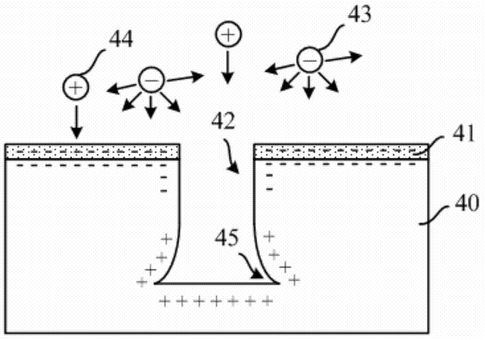
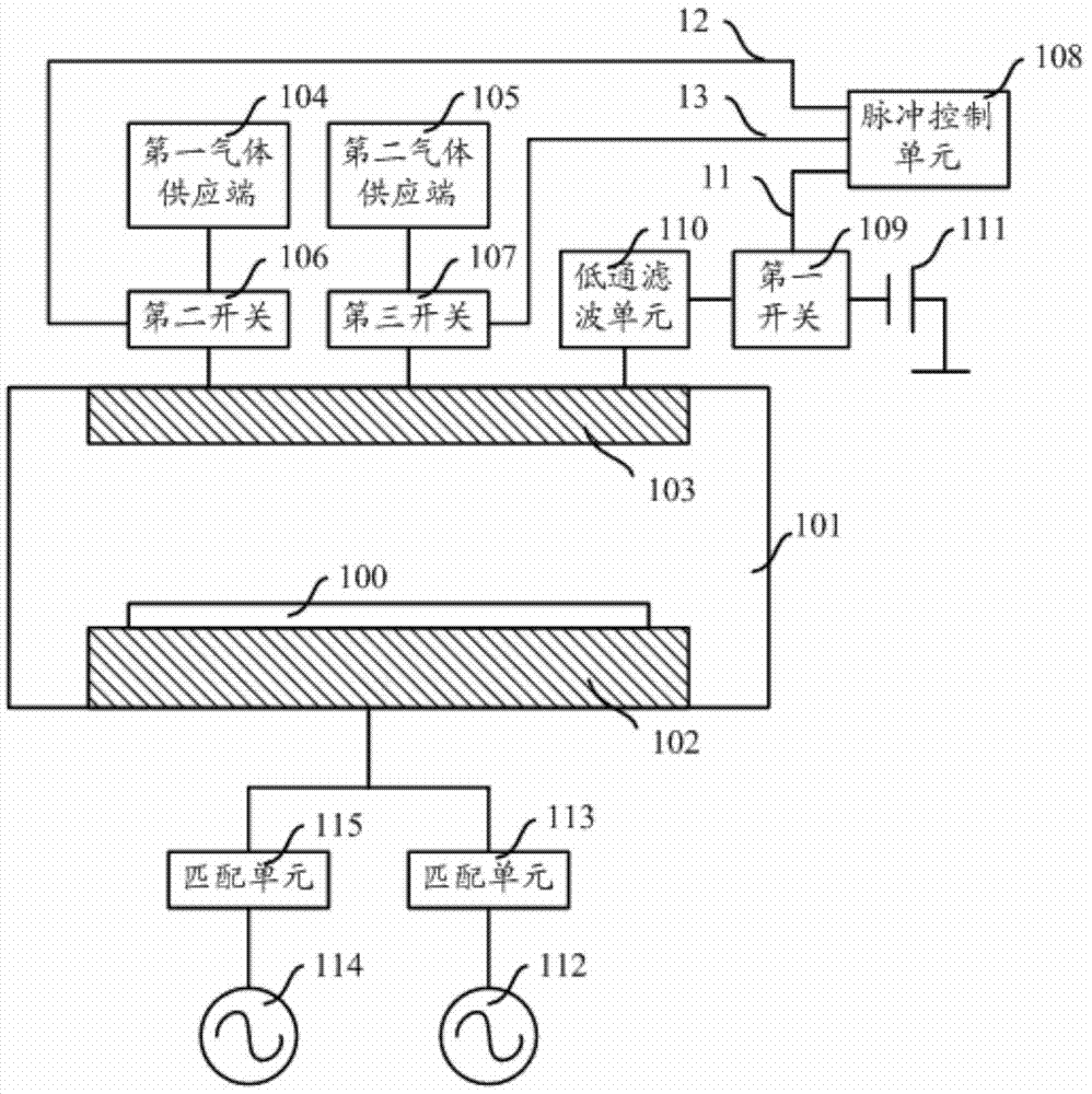
[0045] figure 2 It is a schematic structural diagram of the plasma etching device according to the first embodiment of the present invention.

[0046] refer to figure 2 , the plasma etching device, comprising:

[0047] processing chamber 101;

[0048] The first electrode 102 is located in the processing chamber 101, the first electrode 102 has a platform (not shown) on which the wafer 100 is placed, and the first electrode 102 is electrically connected to at least one radio frequency power supply;

[0049] The second electrode 103 is located in the processing chamber 101 and directly opposite to the first electrode 102, the second electrode 103 is electrically connected to the DC power supply 111, and a first switch 109 is provided between the second electrode 103 and the DC power supply 111;

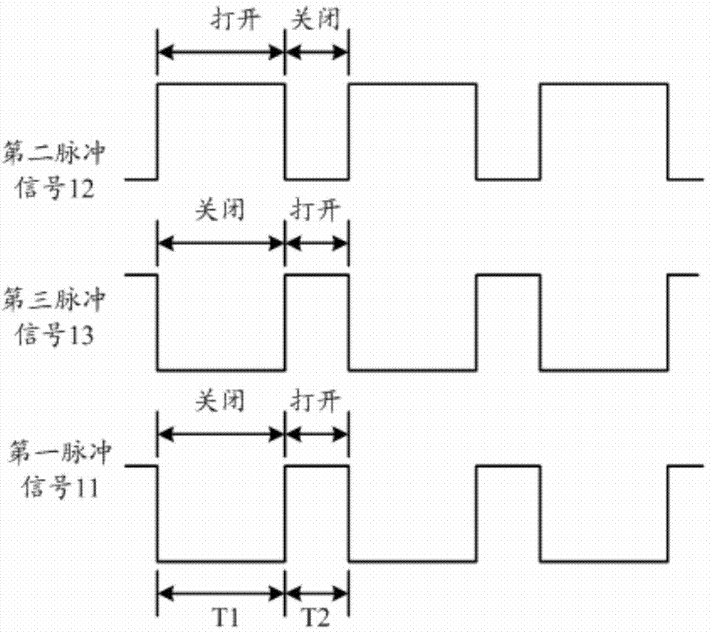
[0050] The first gas supply end 104 is used to introduce the first gas into the processing chamber 101, and there is a second switch 106 between the first gas supply end 104 and th...

no. 2 example

[0078] Figure 5 It is a schematic structural diagram of a plasma etching device according to the second embodiment of the present invention. It should be noted that, for the functions and related limitations of the same structures in the plasma etching apparatus in the second embodiment as in the first embodiment, please refer to the first embodiment, and details will not be repeated in the second embodiment.

[0079] Please refer to Figure 5 , the plasma etching device, comprising:

[0080] processing chamber 201;

[0081] The first electrode 202 is located in the processing chamber 101, the first electrode 202 has a platform for placing the wafer 200, the first electrode 202 is electrically connected to at least one radio frequency power supply, and the first electrode 202 is electrically connected to the DC power supply 221 , there is a first switch 209 between the first electrode 202 and the DC power supply 221;

[0082] The second electrode 203 is located in the pro...


PUM


Abstract

The invention discloses a plasma etching device and an etching method thereof. The plasma etching device comprises a processing chamber, a first electrode, a second electrode, a first gas supply end, a second gas supply end and an impulse control unit, wherein the first electrode is located in the processing chamber, provided with a platform for placing a wafer and electrically connected with at least one radio-frequency power supply; the second electrode is located in the processing chamber, faces the first electrode and is electrically connected with a direct-current power supply, and a first switch is arranged between the second electrode and the direct-current power supply; the first gas supply end feeds first gas into the processing chamber, and a second switch is arranged between the first gas supply end and the processing chamber; the second gas supply end feeds second gas into the processing chamber, and a third switch is arranged between the second gas supply end and the processing chamber; and the impulse control unit synchronously generates a first impulse signal, a second impulse signal and a third impulse signal for controlling the first switch, the second switch and the third switch respectively. The plasma etching device prevents accumulation of electric charge in a to-be-etched material during etching.

Description

technical field [0001] The invention relates to the field of semiconductors, in particular to a plasma etching device and an etching method. Background technique [0002] The semiconductor manufacturing process is a planar manufacturing process, which combines photolithography, etching, deposition, and ion implantation processes. It needs to form a large number of various types of complex devices on the same substrate and connect them to each other to have a complete electronic functions. Among them, deviations in any step of the process may cause the performance parameters of the circuit to deviate from the design values. At present, as the feature size of VLSI devices is continuously reduced and the integration level is continuously improved, higher requirements are put forward for the control of each step of the process and the accuracy of the process results. [0003] Taking the etching process as an example, in the manufacture of integrated circuits, it is often neces...

Claims


Application Information

Patent Timeline
Patent Type & Authority Applications(China)
IPC IPC(8): H01J37/32H01L21/3065
Inventor 尹志尧叶如彬梁洁浦远徐朝阳
Owner ADVANCED MICRO FAB EQUIP INC CHINA
Why Eureka
Try Eureka